
Injection mold, optical component, optical scanning device, and image forming apparatus

Inactive Publication Date: 2014-09-11
RICOH KK
View PDF2 Cites 4 Cited by
  • Summary
  • Abstract
  • Description
  • Claims
  • Application Information

AI Technical Summary

Benefits of technology

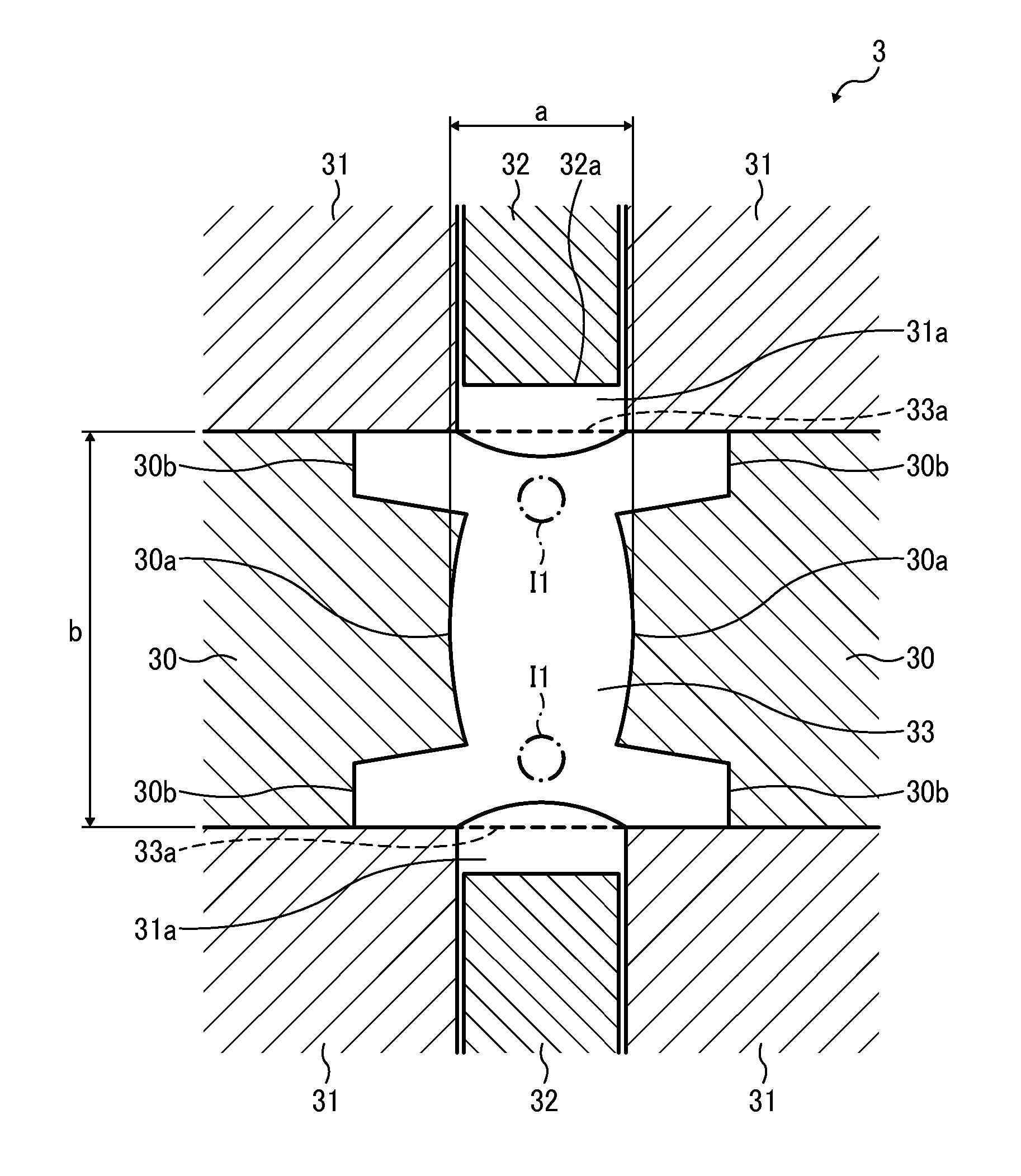
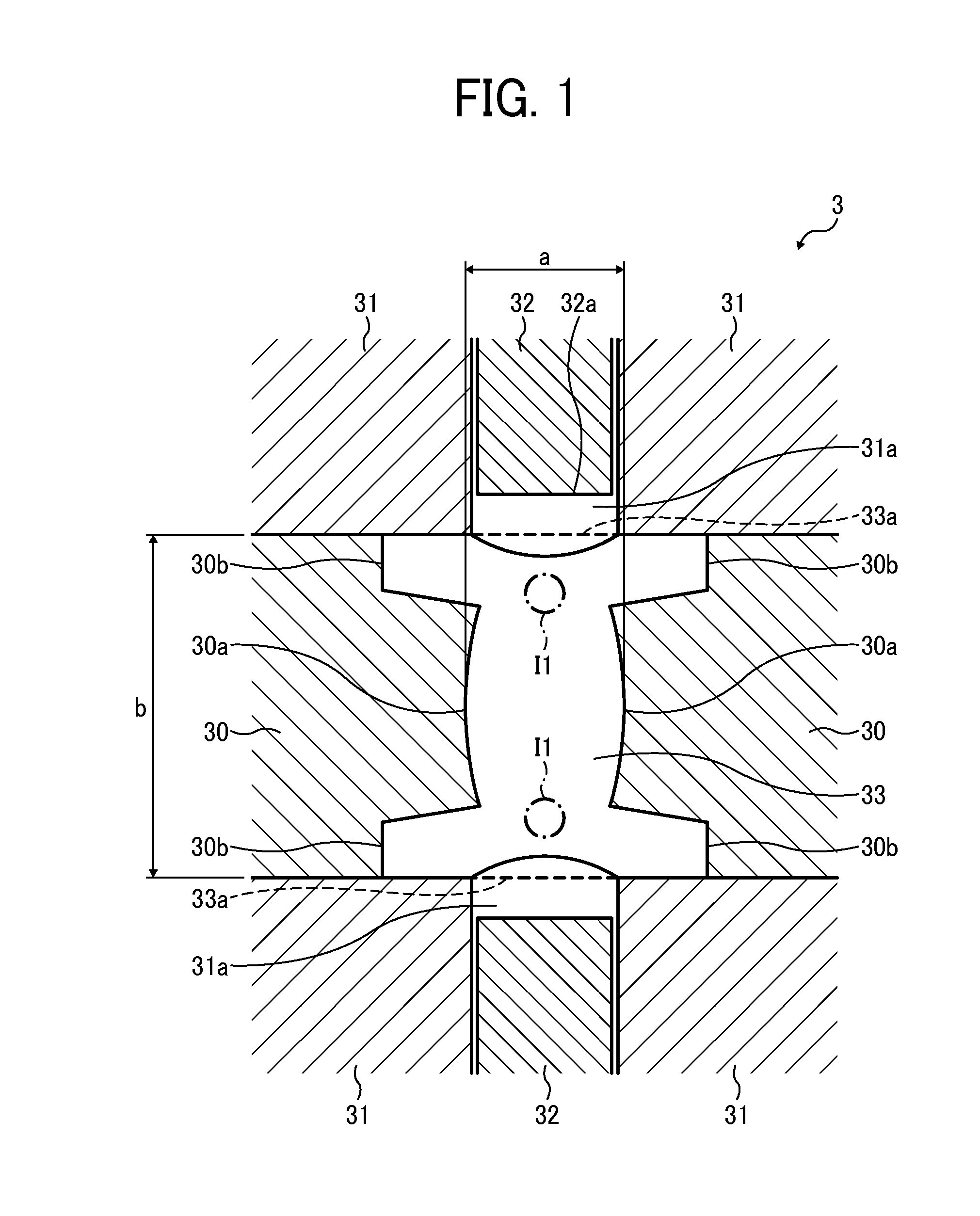
The present invention provides an improved injection mold for molding optical components with a rib on the edge of the optical surface. The mold has a transfer surface for molding the optical surface and a non-transfer surface for molding the non-optical surface. The non-transfer surface is located closer to the rib than the boundary between the transfer surface and the rib. The invention also provides an improved optical component molded in this way, an improved optical scanning device, and an improved image forming apparatus.

Problems solved by technology

Therefore, internal stress generated in the cooling process may cause adhesion of a molded product to the mold or poor release of the molded product from the mold during removal of the molded product from the mold, and also may cause deformation (e.g., warping) of the molded product after the removal of the molded product from the mold.
Particularly, the resin-molded optical component tends to suffer from birefringence due to internal strain.
That is, the lower-pressure injection molding tends to cause sink marks (i.e., surface depressions) in the resin-molded product, reducing the accuracy of transfer of the mold shape.
According to the above-described techniques, however, the air pressure causes internal strain in the resin, increasing the possibility of deformation of the resin-molded product.
A resin-molded optical component subjected to internal strain suffers from significant birefringence.

Method used


Image

  • Injection mold, optical component, optical scanning device, and image forming apparatus
  • Injection mold, optical component, optical scanning device, and image forming apparatus
  • Injection mold, optical component, optical scanning device, and image forming apparatus

Examples


Embodiment Construction

[0033]In describing the embodiments illustrated in the drawings, specific terminology is adopted for the purpose of clarity. However, the disclosure of the present invention is not intended to be limited to the specific terminology so used, and it is to be understood that substitutions for each specific element can include any technical equivalents that have the same function, operate in a similar manner, and achieve a similar result.

[0034]Referring now to the drawings, wherein like reference numerals designate identical or corresponding parts throughout the several views, description will be given of an injection mold, an optical component, an optical scanning device, and an image forming apparatus according to embodiments of the present invention.

[0035]An injection mold according to an embodiment of the present invention will first be described. Description will be given of an example in which the injection mold according to the present embodiment is applied to resin molding of an...


PUM

PropertyMeasurementUnit
Surfaceaaaaaaaaaa

Abstract

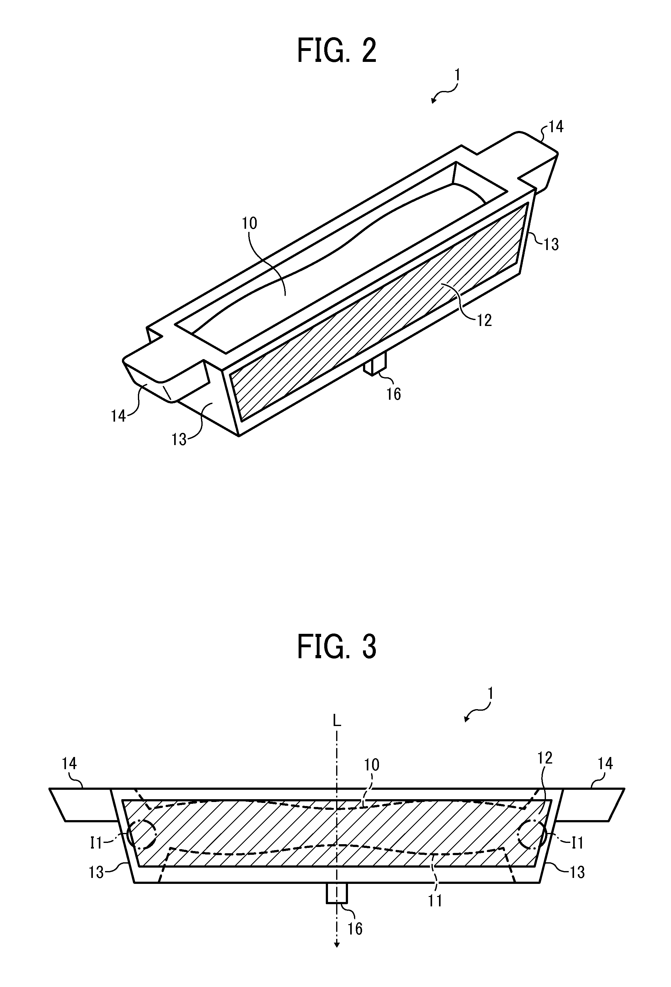
There is provided an injection mold for molding an optical component including an optical surface, a non-optical surface separated from the optical surface, and a rib provided to an edge portion of the optical surface, and longer in a direction parallel to the optical surface than in a direction perpendicular to the optical surface. The mold includes a transfer piece including a transfer surface that molds the optical surface and a movable cavity piece including a non-transfer surface that molds at least a portion of the non-optical surface. The transfer surface and the non-transfer surface define a cavity to be filled with resin. The movable cavity piece is moved away from the resin during a process of cooling the resin. At least a portion of the non-transfer surface is located closer to the rib than a boundary between the transfer surface and the rib.

Description

CROSS-REFERENCE TO RELATED APPLICATION[0001]This patent application is based on and claims priority pursuant to 35 U.S.C. §119 to Japanese Patent Application No. 2013-045063, filed on Mar. 7, 2013, in the Japan Patent Office, the entire disclosure of which is hereby incorporated by reference herein.BACKGROUND[0002]1. Technical Field[0003]The present invention relates to an injection mold for use in injection molding of a resin, an optical component molded in the injection mold, an optical scanning device including the optical component, and an image forming apparatus including the optical scanning device.[0004]2. Related Art[0005]Some optical components of an optical scanning system in an electronic apparatus equipped with an optical scanning device such as a digital laser copier or a laser printer or facsimile machine, optical components of an optical system in an optical device such as a video camera, and optical components such as an optical disc are molded from a resin material....

Claims


Application Information

Patent Timeline
IPC IPC(8): G02B26/12B29C45/00B29C45/26G02B13/00
CPCG02B26/125G02B13/0005B29C45/26B29C45/0025B29C45/37B29L2011/00
Inventor OHHASHI, TAKAMICHIHAYASHI, EIICHIOHTA, YUSUKE
Owner RICOH KK
Learn More