
All-CMOS, Low-voltage, Wide-temperature Range, Voltage Reference Circuit

a voltage reference circuit and low-voltage technology, applied in the field of voltage reference, can solve the problems of high power consumption and large area, difficult to maintain similar temperature drift or td (temperature drift) performance, complex structure, etc., and achieve the effect of simple and effective compensation and minimization of temperature coefficien

Inactive Publication Date: 2014-11-20
UNIVERSITY OF CYPRUS
View PDF5 Cites 7 Cited by
  • Summary
  • Abstract
  • Description
  • Claims
  • Application Information

AI Technical Summary

Benefits of technology

The present invention provides a CMOS voltage reference with resistors that have minimized temperature coefficients. This means that the voltage reference is less affected by changes in temperature.

Problems solved by technology

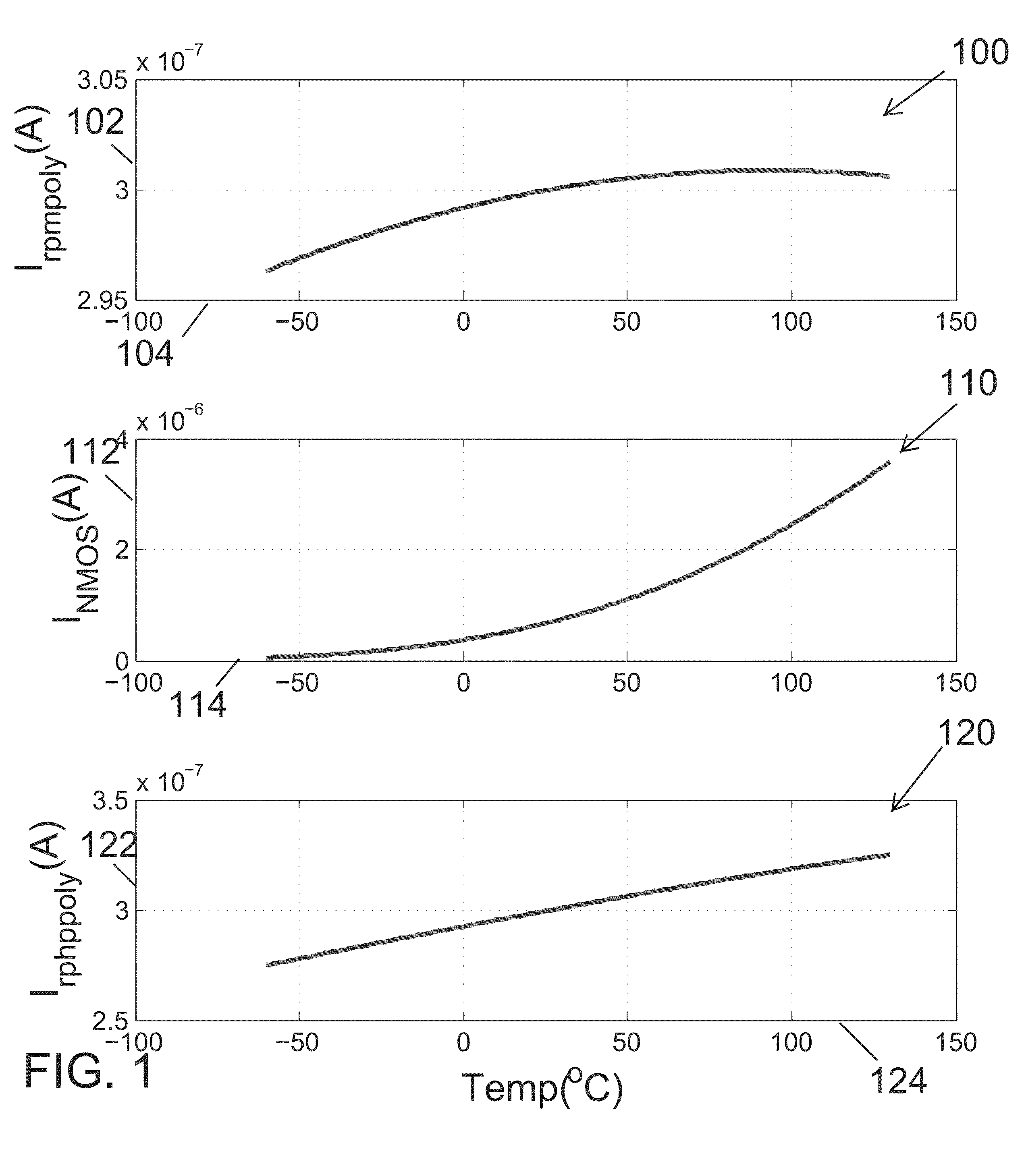
Extending the temperature range beyond commercial applications range, while sustaining similar temperature drift or TD (Temperature Drift) performance, becomes extremely challenging.
Consequently, satisfying all the constraints of modern, high performance applications, is a major challenge which needs alternative and revolutionary methodologies and topologies than previously proposed ones.
These designs are limited by the base-emitter nonlinearities at a TD of approximately 20 ppm / ° C., over a temperature range of approximately 100° C. Alternative proposed topologies provide high order curvature compensation by cancelling part of the nonlinear dependence of a bipolar junction transistors or BJTs base-emitter voltage, although they require complex structures with high power consumption and large area.
This approach has advantages on power consumption and digital process compatibility but suffers from TD performance due to higher non-linearities of MOSFETs compared to bipolar transistors.

Method used


Image

  • All-CMOS, Low-voltage, Wide-temperature Range, Voltage Reference Circuit
  • All-CMOS, Low-voltage, Wide-temperature Range, Voltage Reference Circuit
  • All-CMOS, Low-voltage, Wide-temperature Range, Voltage Reference Circuit

Examples


Embodiment Construction

[0032]Various aspects of the illustrative embodiments will be described utilizing terms commonly employed by those skilled in the art to convey the substance of their work to others skilled in the art. However, it will be apparent to those skilled in the art that the present invention may be practiced with only some of the described aspects. For purposes of explanation, specific numbers, materials and configurations are set forth in order to provide a thorough understanding of the illustrative embodiments. However, it will be apparent to one skilled in the art that the present invention may be practiced without the specific details. In other instances, well-known features are omitted or simplified in order not to obscure the illustrative embodiments.

[0033]Various operations will be described as multiple discrete operations, in turn, in a manner that is most helpful in understanding the present invention. However, the order of description should not be construed as to imply that thes...


PUM


Abstract

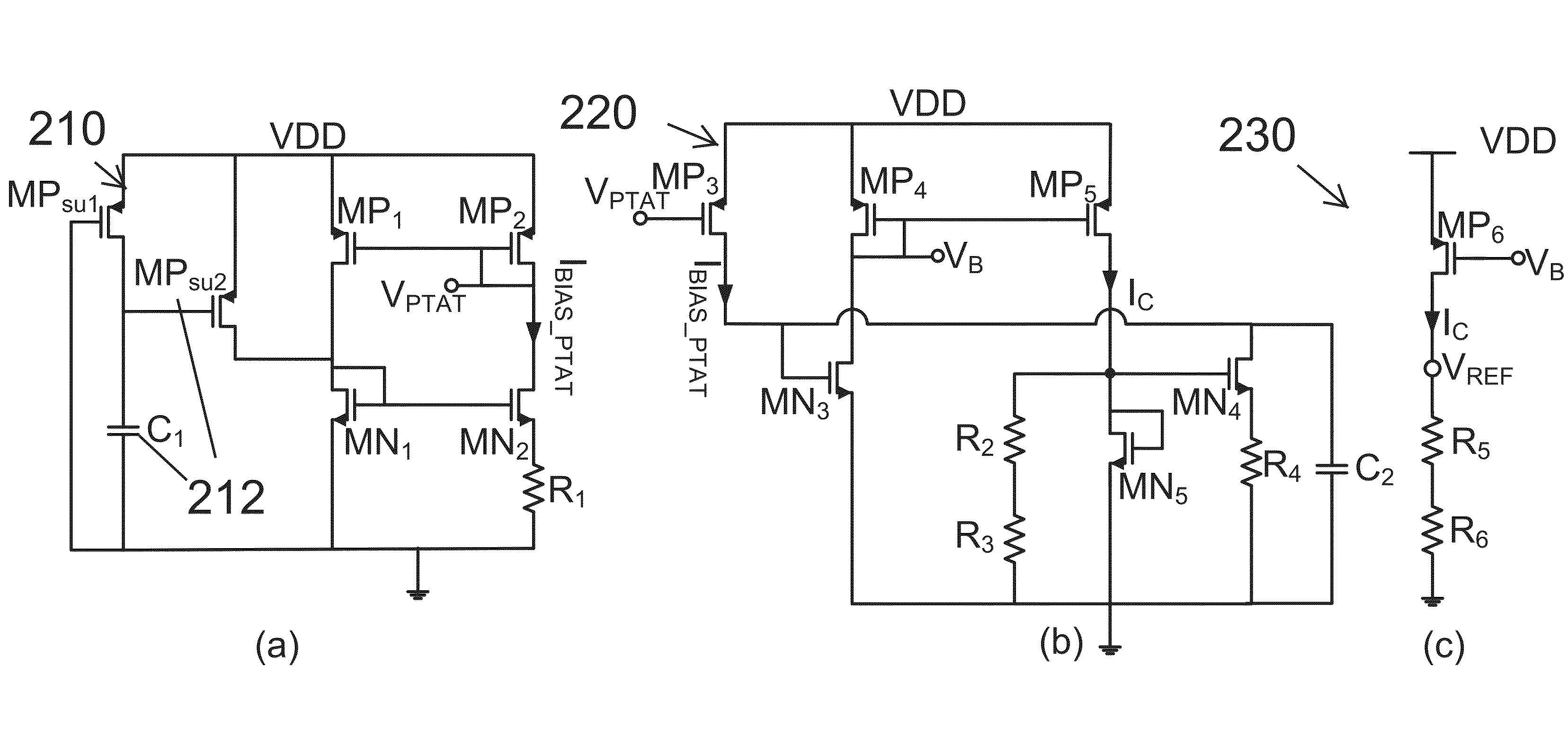
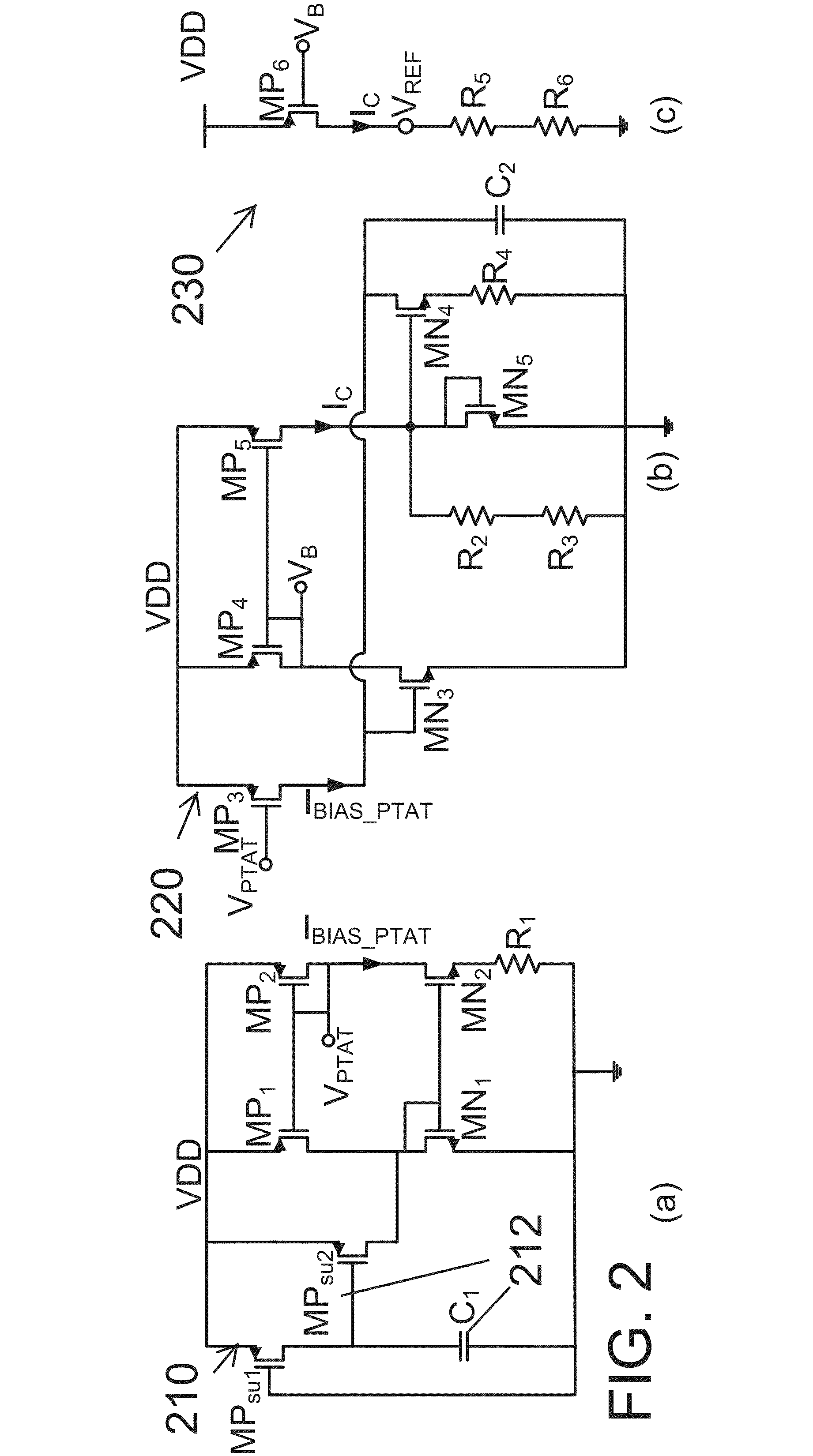
A CMOS voltage reference is disclosed. The CMOS voltage reference may include a PTAT current bias circuit including a start-up circuit, a core module implementing high order non-linear curvature compensation and an output stage supplying the reference voltage. The CMOS voltage reference may include a PTAT current bias circuit having a start-up and a CTAT feedback loop and a PTAT feedback loop and a compensating circuit summing the current from the CTAT feedback loop and the PTAT feedback loop.

Description

[0001]This application claims priority to U.S. Provisional Application 61 / 825,086 filed on May 19, 2013, the entire disclosure of which is incorporated by reference.BACKGROUND OF THE INVENTION[0002]1. Field of the Invention[0003]The present invention is a voltage reference. More specifically, the present invention is a complementary metal oxide semiconductor or CMOS voltage reference.[0004]2. Description of the Related Art[0005]High performance voltage references are sine qua non in a system design due to the necessity of supplying, a temperature and voltage insensitive reference to many analog, digital and mixed signal circuits such as operational amplifiers, sensors, flash memories, digital-to-analog converters or DACs, filters and regulators. The accuracy and robustness of the reference voltage will undoubtedly be of major importance if the resolution of the subsequent circuits is to have any significance in the system level. Extending the temperature range beyond commercial appl...

Claims


Application Information

Patent Timeline
IPC IPC(8): G05F3/16
CPCG05F3/16G05F3/24G05F3/245
Inventor GEORGIOU, JULIUSANDREOU, CHARALAMBOS
Owner UNIVERSITY OF CYPRUS
Learn More