

Avalanche protection for wide bandgap devices
- Summary
- Abstract
- Description
- Claims
- Application Information
AI Technical Summary
Benefits of technology
Problems solved by technology
Method used
Image

Examples
Embodiment Construction
[0028] Multi-die semiconductor packages are well known in the art, and are generally described in U.S. Pat. Nos. 6,40,050; 6,297,55; 6,113,632; and 5,814,884; all issued to Davis et. al., and which are each incorporated herein by reference.
[0029] The method of the present invention is accomplished by paralleling a clamping device having a lower reverse breakdown voltage BV with a wide bandgap device, such that reverse transient energy is absorbed by the clamping device. The clamping device must maintain a BV during avalanche less than the wide bandgap diode. To prevent conduction through the clamping device when the wide bandgap device is forward biased, the clamping device must have a higher voltage drop than the wide bandgap device.
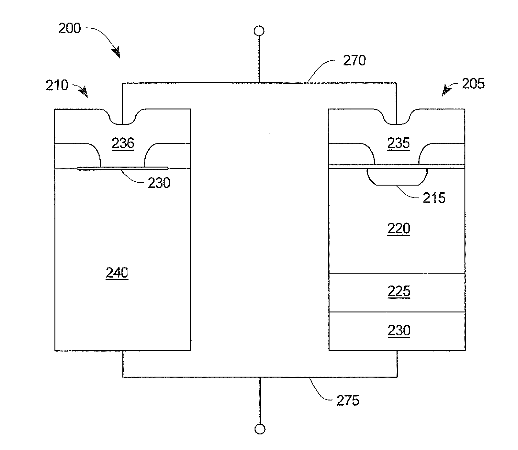
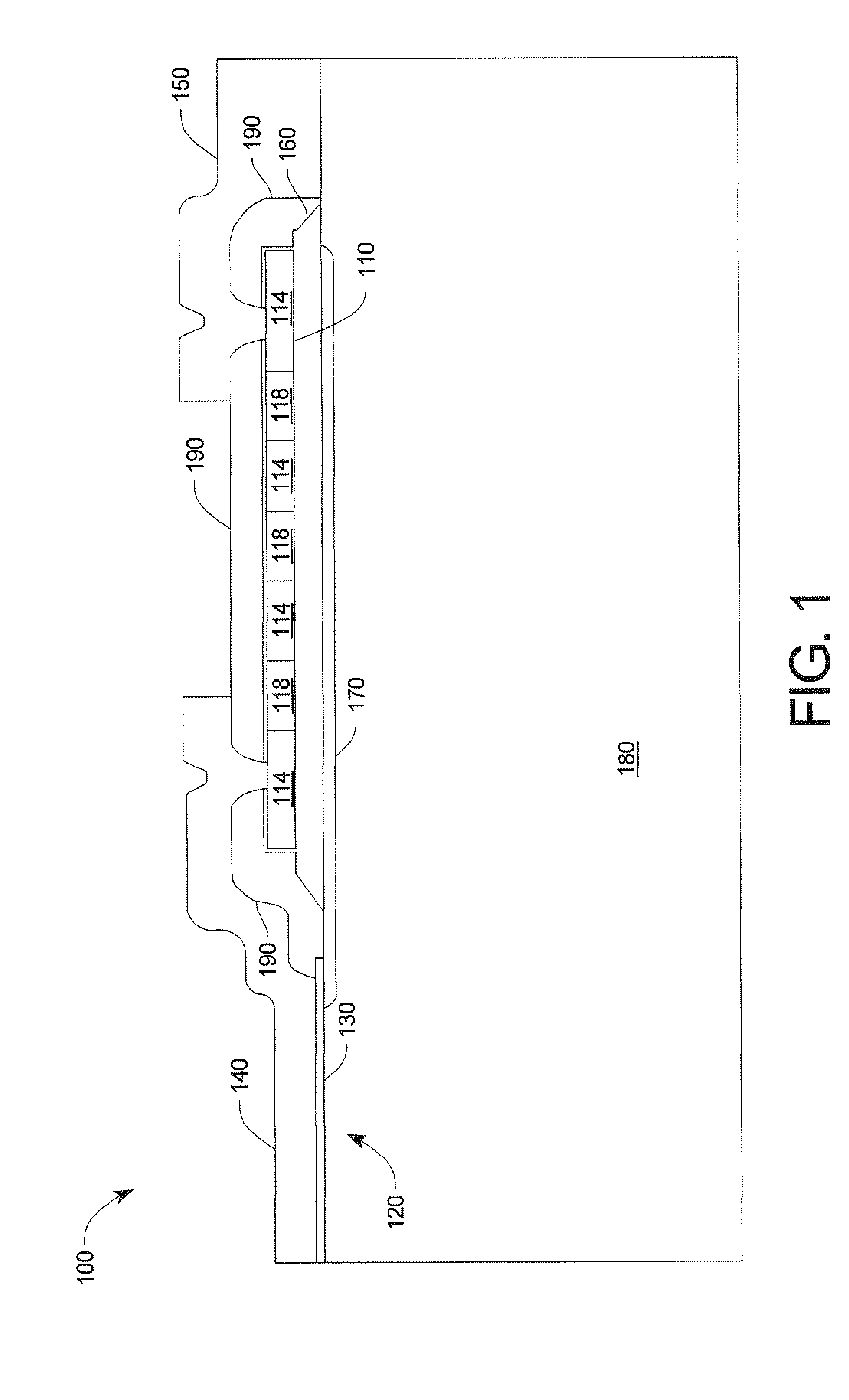
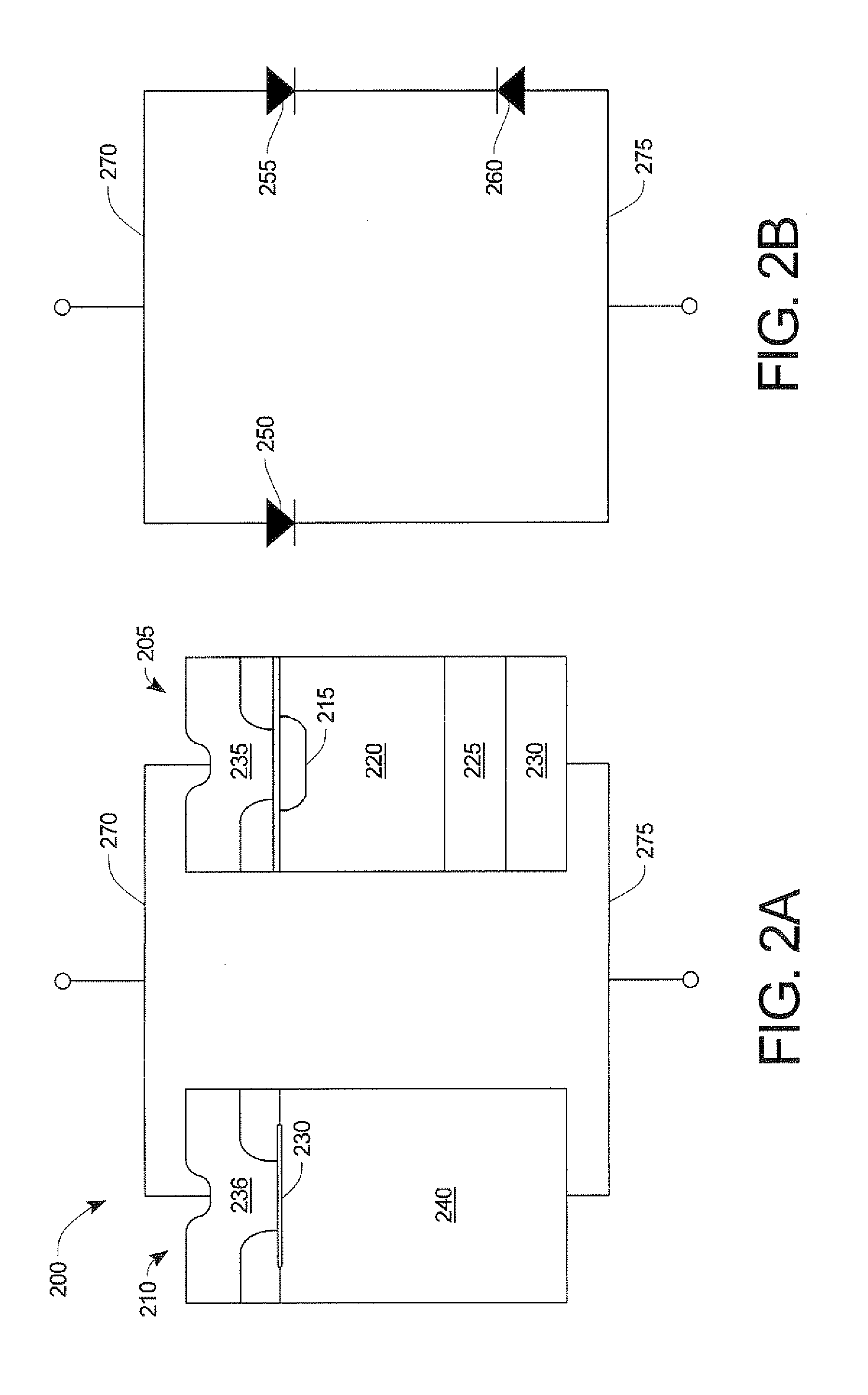
[0030] Referring to FIG. 1, there is shown one embodiment 100 of a wide bandgap device consisting of a SiC Schottky diode 120 and a clamping device 110 according to the present invention. The improvement in wide bandgap avalanche capability is achieve...
PUM
 Abstract
Description
Claims
Application Information