
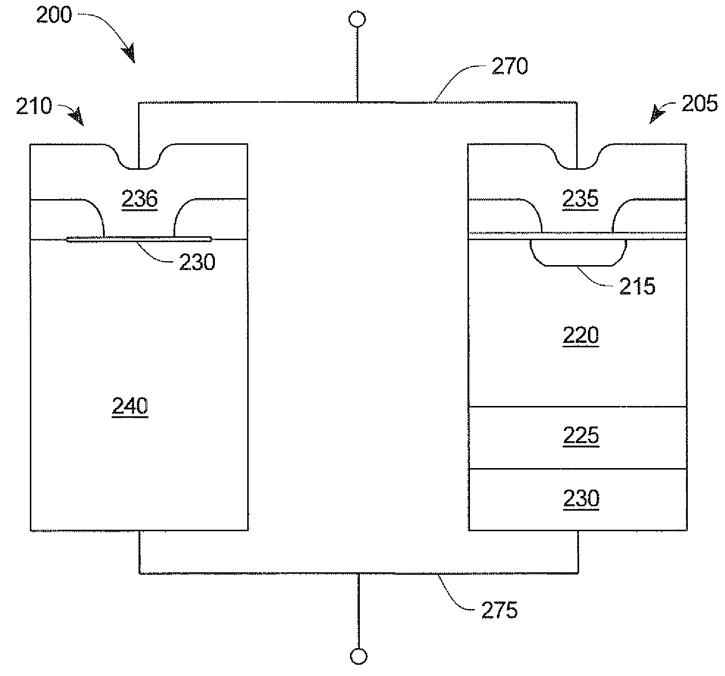
Wide bandgap device in parallel with a device that has a lower avalanche breakdown voltage and a higher forward voltage drop than the wide bandgap device

a wide bandgap device and wide bandgap technology, applied in semiconductor devices, semiconductor/solid-state device details, diodes, etc., can solve the problems of poor and erratic avalanche capability of wide bandgap devices, almost always destructive, and destroy devices, so as to optimize the pnp gain and minimize the temperature coefficient

Active Publication Date: 2009-09-08
SEMICON COMPONENTS IND LLC
View PDF14 Cites 8 Cited by
  • Summary
  • Abstract
  • Description
  • Claims
  • Application Information

AI Technical Summary

Benefits of technology

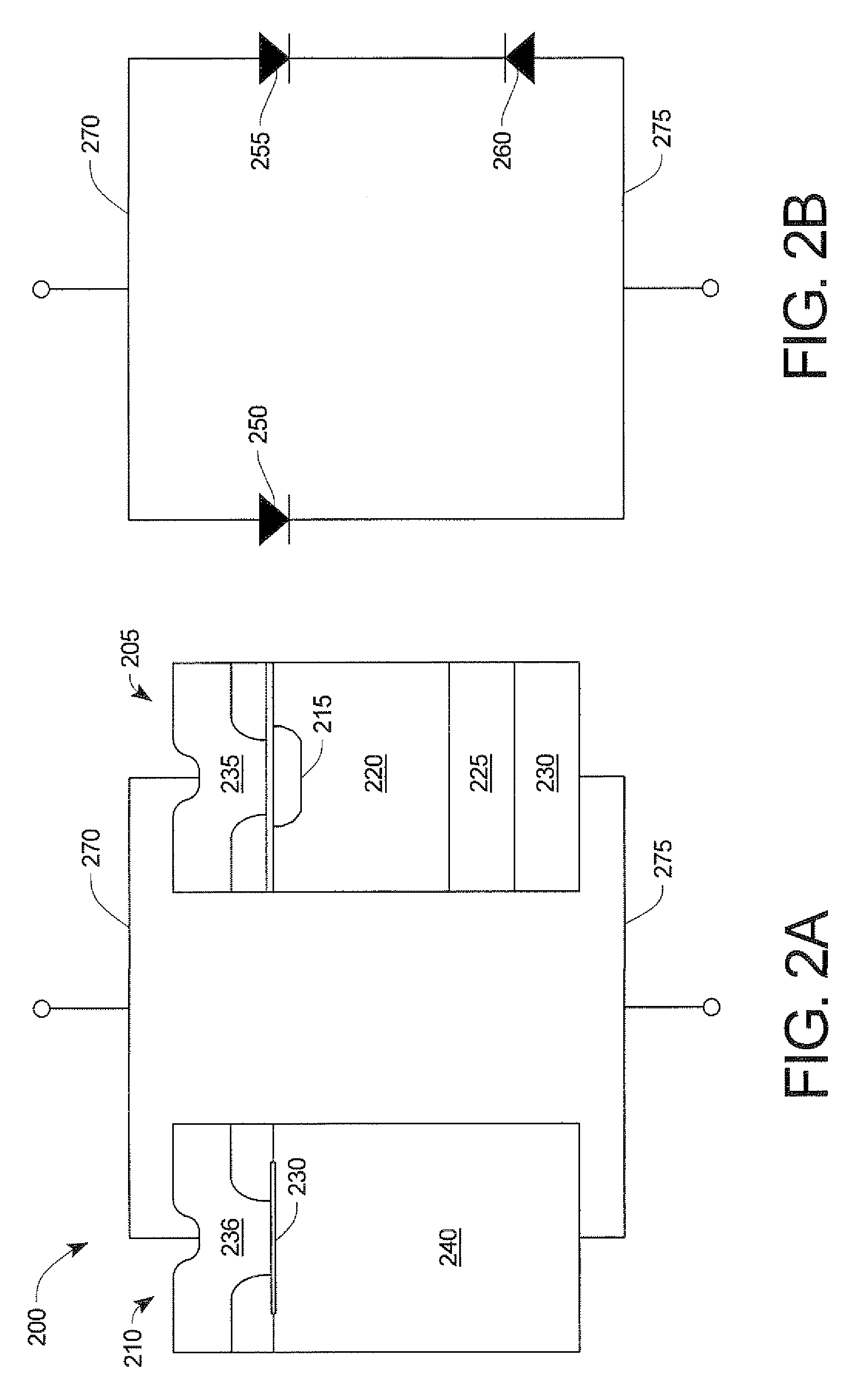
The invention is about improving the performance of wide bandgap devices by adding a multiple series of diodes across the blocking junction of a wideband gap device. This helps to increase the avalanche capability of the device. The invention also includes a silicon vertical PNP transistor and a method for protecting wide bandgap devices from failing during suppression of voltage transients. The clamping device used in the method has a higher forward voltage drop, which prevents forward conduction and reduces degradation of switching speed. The invention also uses a simple vertical open base transistor and optimizes PNP gain by controlling the peak buffer concentration and charge to minimize the temperature coefficient of collector-to-emitter breakdown. Overall, the invention allows for improved performance and reliability of wide bandgap devices.

Problems solved by technology

However, wide bandgap devices (e.g., silicon carbide) have poor and erratic avalanche capability due to starting substrate quality.
This phenomenon can be quite useful in semiconductor diodes such as the avalanche diode and avalanche photodiode, but in other situations, such as in MOSFET transistors, avalanche breakdown can destroy the device.
When avalanche breakdown occurs within a solid insulating material it is almost always destructive.
If the voltage increases beyond the design limit, the diode undergoes avalanche breakdown, limiting the harmful voltage.
Paralleling a simple zener diode with the wide bandgap device can result in the injection of minority carriers in the wide bandgap device, thus degrading the switching performance of the wide bandgap device.

Method used


Image

  • Wide bandgap device in parallel with a device that has a lower avalanche breakdown voltage and a higher forward voltage drop than the wide bandgap device
  • Wide bandgap device in parallel with a device that has a lower avalanche breakdown voltage and a higher forward voltage drop than the wide bandgap device
  • Wide bandgap device in parallel with a device that has a lower avalanche breakdown voltage and a higher forward voltage drop than the wide bandgap device

Examples


Embodiment Construction

[0026]Multi-die semiconductor packages are well known in the art, and are generally described in U.S. Pat. Nos. 6,40,050; 6,297,55; 6,113,632; and 5,814,884; all issued to Davis et. al., and which are each incorporated herein by reference.

[0027]The method of the present invention is accomplished by paralleling a clamping device having a lower reverse breakdown voltage BV with a wide bandgap device, such that reverse transient energy is absorbed by the clamping device. The clamping device must maintain a BV during avalanche less than the wide bandgap diode. To prevent conduction through the clamping device when the wide bandgap device is forward biased, the clamping device must have a higher voltage drop than the wide bandgap device.

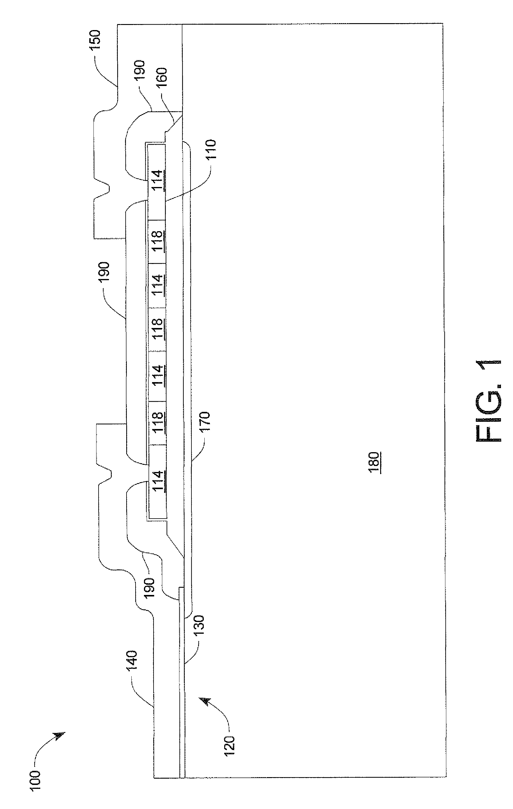
[0028]Referring to FIG. 1, there is shown one embodiment 100 of a wide bandgap device consisting of a SiC Schottky diode 120 and a clamping device 110 according to the present invention. The improvement in wide bandgap avalanche capability is achieved by ...


PUM


Abstract

A wide bandgap device in parallel with a device having a lower avalanche breakdown voltage and a higher forward voltage drop than the wide bandgap device.

Description

CROSS-REFERENCE TO RELATED APPLICATIONS[0001]This application claims priority from U.S. Provisional Patent Application Ser. No. 60 / 833,362, filed on Jul. 26, 2006, which application is hereby incorporated by reference.FIELD OF THE INVENTION[0002]This invention relates to semiconductor devices, and more specifically, to a method and device for protecting wide bandgap diodes from failing during suppression of voltage transients.BACKGROUND OF THE INVENTION[0003]Wide bandgap (“WBG”) semiconductors are emerging as materials capable of driving continued device performance enhancements for many years to come. These materials are typically defined as exhibiting an electronic bandgap greater than 2 eV. Silicon Carbide (SiC) has been studied for decades, but recent developments have firmly established SiC commercial products in optical, RF, and power components. With extremely high thermal and chemical stability, and electrical performance, WBG devices are used for high frequency, high temper...

Claims


Application Information

Patent Timeline
Patent Type & Authority Patents(United States)
IPC IPC(8): H01L27/02
CPCH01L27/0248H01L29/872H01L29/87H01L29/8618H01L29/1608H01L29/70H01L31/0312
Inventor YEDINAK, JOSEPH A.WOODIN, RICHARD L.REXER, CHRISTOPHER LAWRENCESHENOY, PRAVEEN MURALEEDHARANOH, KWANGHOONYUN, CHONGMAN
Owner SEMICON COMPONENTS IND LLC
Learn More