Supercharge Your Innovation With Domain-Expert AI Agents!

Backplane of flat panel display and method of manufacturing the same

a flat panel display and backplane technology, applied in the direction of identification means, instruments, semiconductor devices, etc., can solve the problems of surface film rupture at the backplane of the display device, damage such as surface film rupture, and the damage of the transparent materials for forming the transparent display device is often damaged

Active Publication Date: 2014-12-25
SAMSUNG DISPLAY CO LTD
View PDF3 Cites 14 Cited by
  • Summary
  • Abstract
  • Description
  • Claims
  • Application Information

AI Technical Summary

Benefits of technology

The present invention relates to a backplane for a flat panel display device that is resistant to high temperature processes. The method of manufacturing the backplane includes forming an insulation substrate on a glass substrate, forming a protection layer on the insulation substrate, and forming a transistor on the protection layer. The method also includes forming a first hole in the insulation substrate, filling the first hole with a material, and forming a pixel electrode on the insulation substrate. The backplane includes an insulation substrate with a transistor area and a non-transistor area, and a first insulating layer covering the transistor area. The first insulating layer includes a second hole exposing a portion of the source electrode or drain electrode. The method and the backplane provide improved resistance to high temperature processes and improved performance of the flat panel display device.

Problems solved by technology

However, some of the transparent materials for forming the transparent display device are often damaged at higher temperatures.
For example, damage such as a surface film rupture at the backplane of the display device may occur due to an outgassing phenomenon at a high temperature.

Method used


Image

  • Backplane of flat panel display and method of manufacturing the same
  • Backplane of flat panel display and method of manufacturing the same
  • Backplane of flat panel display and method of manufacturing the same

Examples


Embodiment Construction

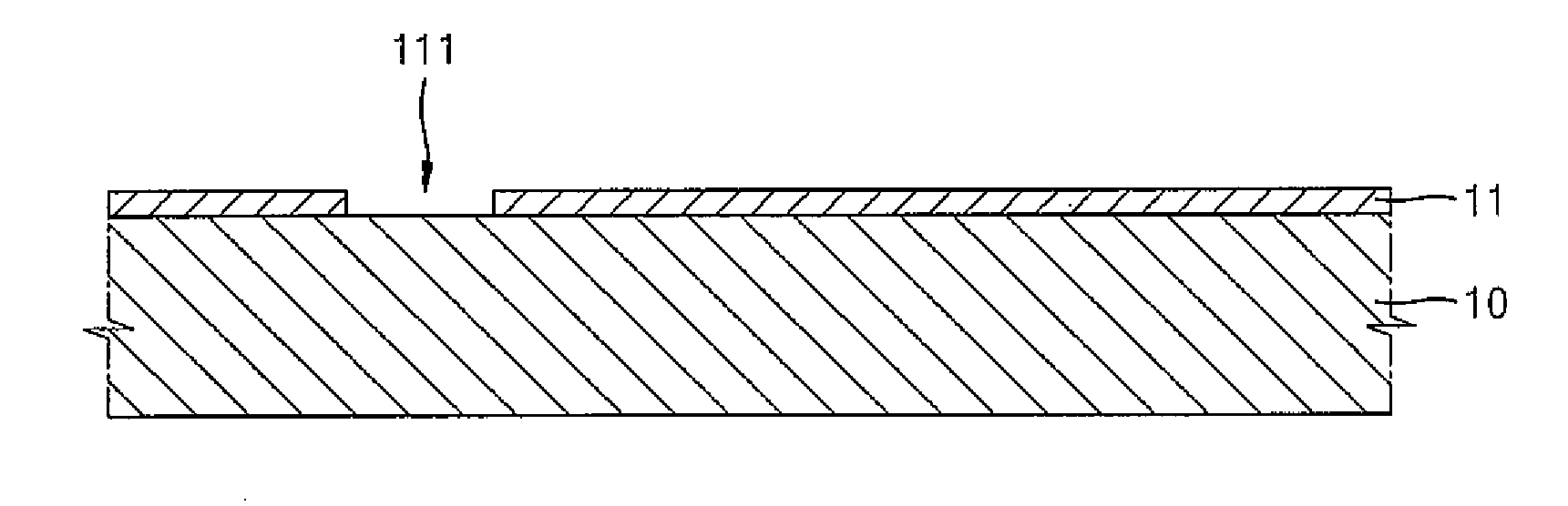
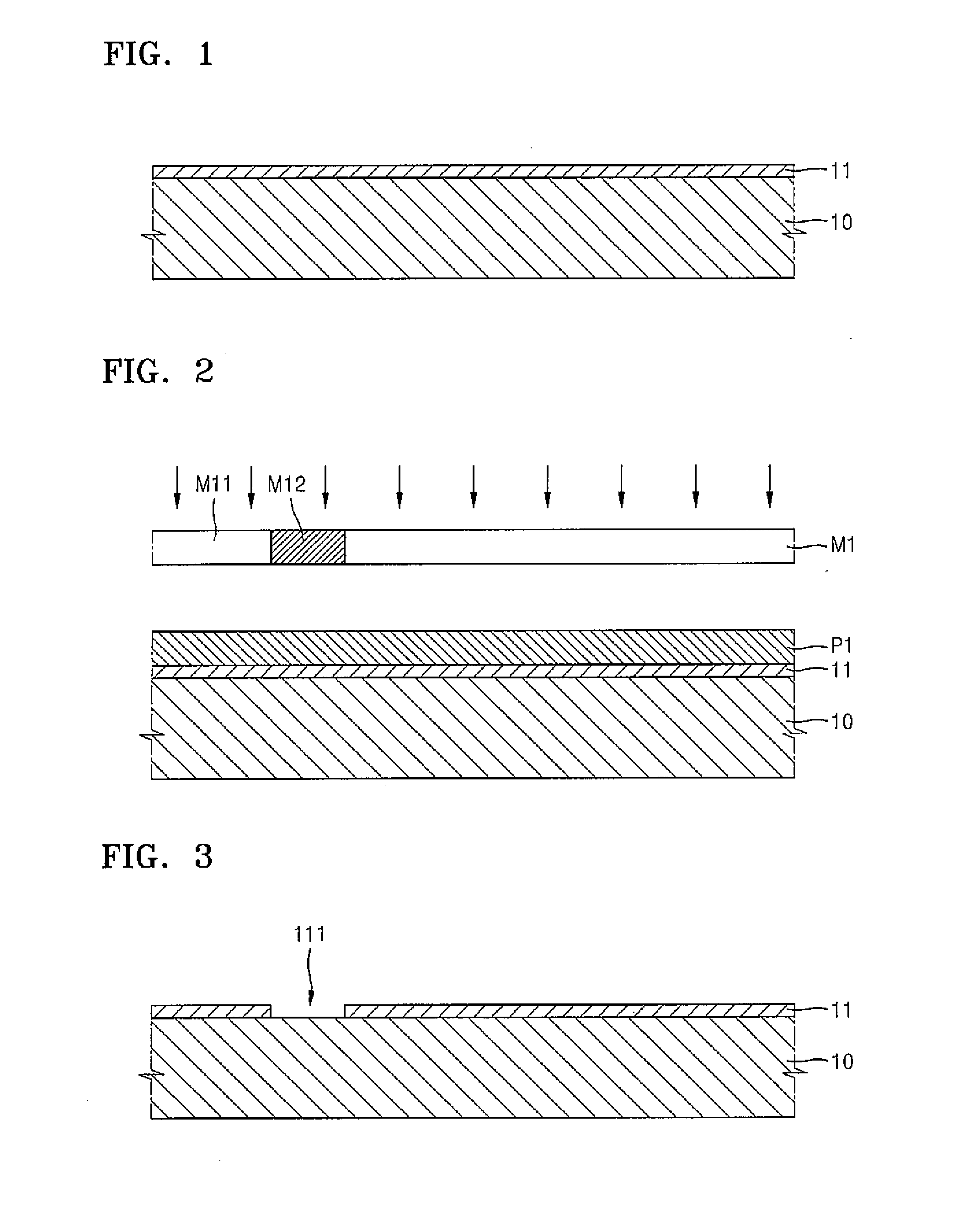
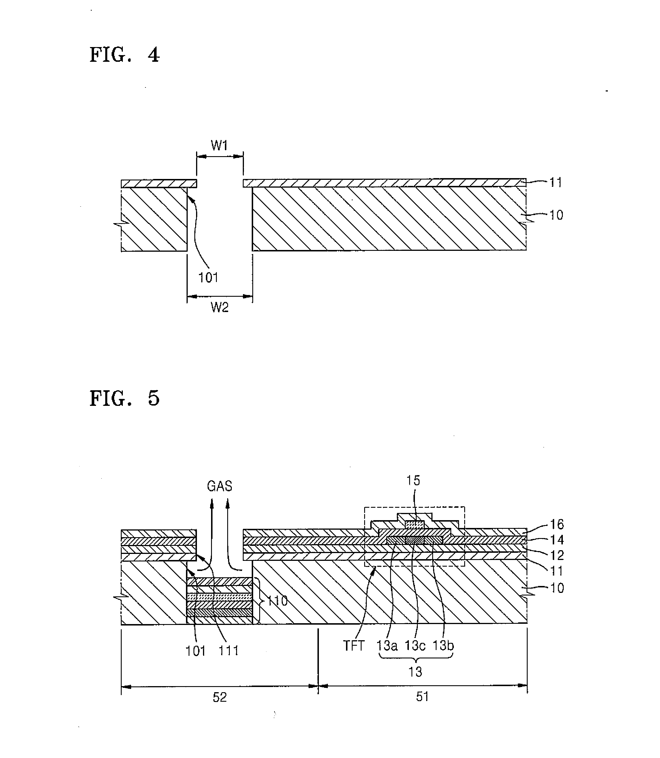
[0041]As the present invention allows for various changes and numerous embodiments, embodiments will be illustrated in the drawings and described in detail in the description. However, this is not intended to limit the present invention to a particular mode of practice, and it is to be appreciated that the present invention encompasses all changes, equivalents, and substitutes that do not depart from the spirit and technical scope thereof. In the description of the present invention, well-known methods will not be described in detail so as not to unnecessarily obscure the essence of the present invention.

[0042]While terms such as “first” and “second” may be used to describe various components, such components must not be limited to the above terms. The terms are used only to distinguish one component from another.

[0043]The terms used in the present application are merely used to describe an embodiment, and are not intended to limit the present invention. Use of singular forms includ...


PUM


Abstract

Provided are a backplane for a flat panel display device and a method of manufacturing the backplane. The method of manufacturing the backplane for a flat panel display device includes forming an insulation substrate on a glass substrate, forming a protection layer on the insulation substrate, the protection layer including a first opening exposing a portion of the insulation substrate, forming a first hole in the insulation substrate by removing the portion of the insulation substrate exposed by the first opening, and forming a transistor on the protection layer, the transistor including an active layer, a gate electrode, a source electrode, and a drain electrode. The insulation substrate may include a transistor area including the transistor, and a non-transistor area excluding the transistor and including the first hole.

Description

CROSS-REFERENCE TO RELATED APPLICATION[0001]This application claims priority to and the benefit of Korean Patent Application No. 10-2013-0071159, filed on Jun. 20, 2013, in the Korean Intellectual Property Office, the disclosure of which is incorporated herein in its entirety by reference.BACKGROUND[0002]1. Field[0003]The present invention relates to a backplane for a flat panel display and a method of manufacturing the same.[0004]2. Description of the Related Art[0005]A flat panel display device, such as an organic light-emitting display (OLED) device or a liquid crystal display (LCD) device, includes a backplane having at least one thin-film transistor (TFT). The TFT includes an active layer, which provides a channel area, a source area, and a drain area, and a gate electrode that is formed on the channel area and is electrically insulated from the active layer by a gate insulating layer.[0006]The active layer of such a TFT may be formed of a semiconductor material, such as amorph...

Claims


Application Information

Patent Timeline
IPC IPC(8): H01L27/12
CPCH01L27/127H01L27/1222H01L27/1262H01L27/1218H10K59/88H10K59/1201G09F9/00H10K59/123H10K59/124H10K59/1213H10K59/126H01L27/1259H10K59/00H10K59/12
Inventor KIM, JONG-YUNYU, CHEOL-HO
Owner SAMSUNG DISPLAY CO LTD
Features
  • R&D
  • Intellectual Property
  • Life Sciences
  • Materials
  • Tech Scout
  • Unparalleled Data Quality
  • Higher Quality Content
  • 60% Fewer Hallucinations
Learn More