

Method and apparatus for imaging an object
- Summary
- Abstract
- Description
- Claims
- Application Information
AI Technical Summary
Benefits of technology
Problems solved by technology
Method used
Image

Examples
first embodiment
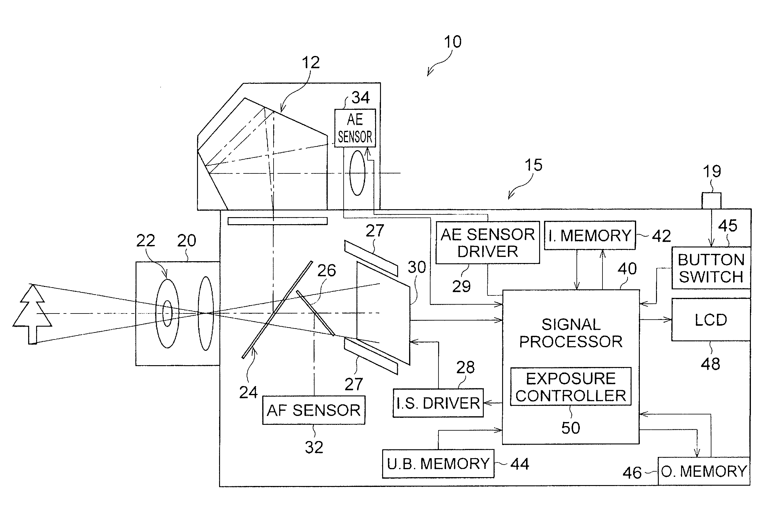
[0033]FIG. 1 is a block diagram of a digital camera according to the
[0034]An SLR-type digital camera 10 is equipped with a body 15 and a photographing optical system 20 detachably attached to the body 15. A user can select and set a mode from various modes such as a photography mode, a replay mode, etc., by operating a mode dial or mode button (not shown). When electric power is turned on, the photography mode is set.
[0035]Light reflected off a target subject enters into the photographing optical system 20 and an iris 22, and a portion of the light is directed to an optical finder 12 by a quick return mirror 24. Also, a portion of the light passes through the quick return mirror 24 and is directed to an AF sensor 32 by a half mirror 26.
[0036]The optical finder 12 forms light that entered the optical finder 12 so that a user can confirm an object image via an eyepiece lens (not shown). Also, an AE sensor 34 is disposed near to the optical finder 12 and an object image is formed on a ...
third embodiment
[0071]FIG. 9 is a view illustrating a pixel addition process according to the
[0072]In FIG. 9, part of a 6×4 pixel array 134′R in the AE sensor is illustrated. A color filter array 135′ is disposed on the AE sensor 134′ and the color filter elements 135′ R, G1, G2, and B are arrayed in the horizontal direction, i.e., the row direction in each color. Then, a pixel addition process using different numbers of pixel addition is performed with respect to the row direction.
second embodiment
[0073]Concretely speaking, the number of pixel addition “2” is applied to neighboring pixel areas R2 and R4 along the column direction, and the number of pixel addition “1” is applied to pixel areas R2 and R3 located between the pixel areas R1 and R4. Consequently, four image-pixel signals “A1′-A4′” along the row direction are read out. The AE sensor 134 has switch circuits that are the same as those shown in FIG. 7 according to the The switch circuits allows neighboring image-pixel signals along the column to be mixed, and a pixel addition process based on the number of pixel addition “1” and the number of pixel addition “2” is performed. Note that, when the AE sensor 134 is a CCD image sensor, a pixel addition process along the column is performed by utilizing a horizontal transfer circuit.
[0074]FIGS. 10A and 10B illustrate a pixel addition process along the row and column directions, respectively.
[0075]Herein, a pixel addition process based on different numbers of pixel addition...
PUM
 Abstract
Description
Claims
Application Information