Address mapped repartitioned digital pixel

a digital pixel and address mapping technology, applied in the field of read out circuits of detector arrays, can solve the problems of high system cost of implementing the same function and level of performance with off-device logic, as in conventional frame summing, and achieve the effects of avoiding extrapolation errors, robust image stabilization, and improving stabilization accuracy

Active Publication Date: 2015-04-30
RAYTHEON CO
View PDF0 Cites 39 Cited by
  • Summary
  • Abstract
  • Description
  • Claims
  • Application Information

AI Technical Summary

Benefits of technology

[0021]Application of address mapping to the accumulated sub-frame allows for on-FPA stabilization at sub-frame rates. The address mapping for accumulated sub-frames may be a generalized mapping configured to accommodate small or large shifts, roll, magnification, polynomial warp or keystone correction. In some embodiments, the sub-frame address mapping may be limited to a non-isomorphic mapping that excludes linear shifts. Because quantization events are accumulated before they are further accumulated into a sub-frame, sub-frame motion can be measured a posteriori, before the sub-frame address mapping is applied, avoiding extrapolation error and improving stabilization accuracy.
[0022]In some embodiments, address mapping is applied to both the quantization events and accumulated sub-frames. Address mapping may be applied to the quantization events at a high update rate to align data in the quantization memory as the digital values for reported quantization events are accumulated. This mapping may be confined to small shifts. Address mapping may be app

Problems solved by technology

The system cost of implementing the same function and level of performance with

Method used


Image

  • Address mapped repartitioned digital pixel
  • Address mapped repartitioned digital pixel
  • Address mapped repartitioned digital pixel

Examples


first embodiment

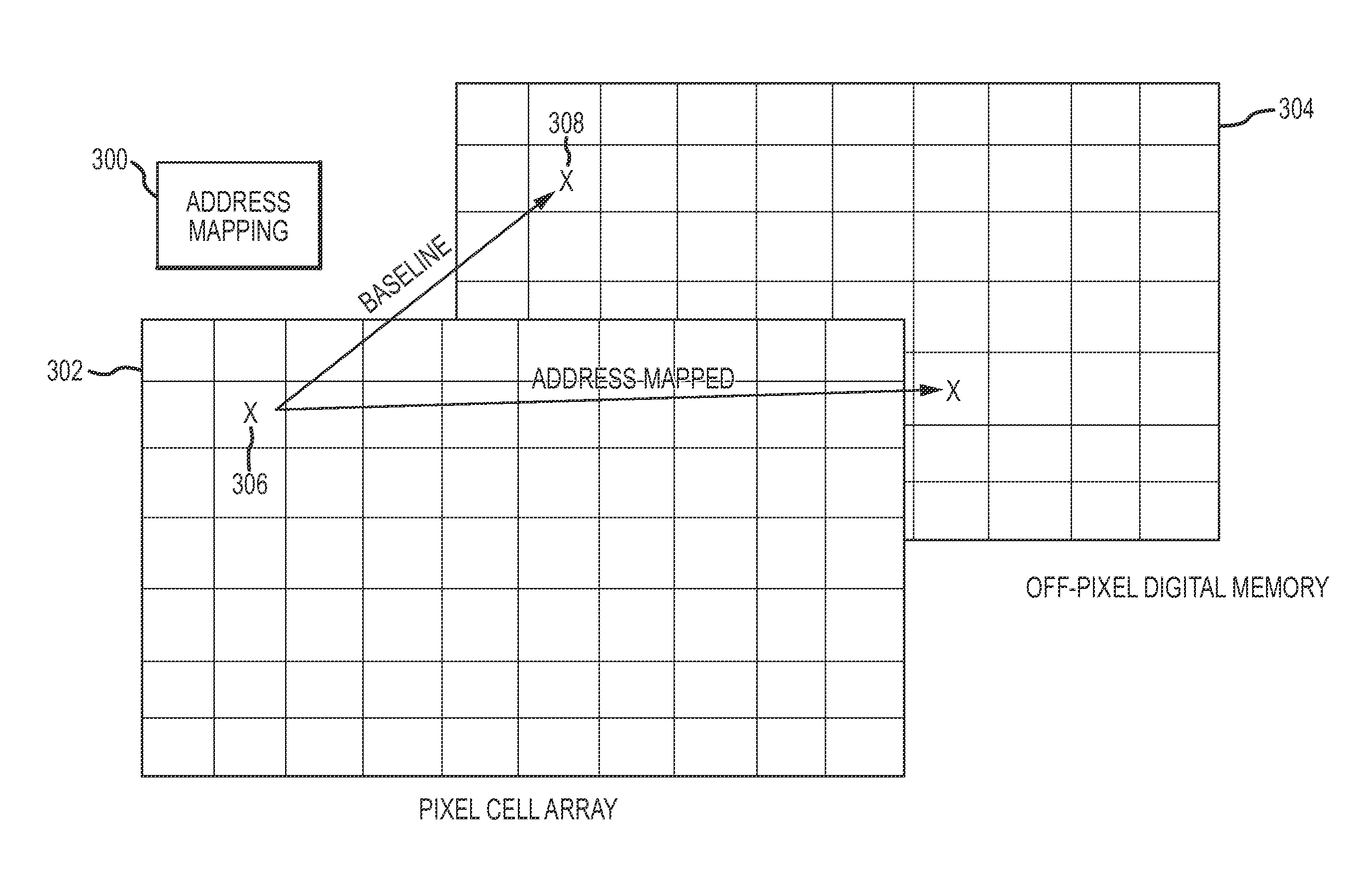
[0092]More particularly, in a first embodiment, the digital values for the selected quantization events are accumulated into a first temporary frame. The accumulated digital values for the just completed sub-frame are read out and added to the addressed mapped memory location in frame memory while the digital values for the next selected quantization events are accumulated into a second temporary frame while the digital values in the first temporary frame are distributed to the registered memory locations in frame. This continues by ping ponging between the first and second temporary frames. At the end of the integration period, the registered memory locations are output and frame residuals are and output separately.

second embodiment

[0093]In a second embodiment, the digital values for the selected quantization events are accumulated into a temporary frame. The accumulated digital values for the just completed sub-frame are read out and added to the addressed mapped memory location in frame memory. The digital values in the temporary frame are distributed to the registered memory locations in frame and the process repeats. At the end of the integration period, the registered memory locations are output and frame residuals are and output separately.

[0094]Major simplifications of the SF address mapping logic may be achieved by calculating pixel addresses in sequence. For example, the logic keeps track of address and intermediate values for the pixel denoted P(r,c), where “r” is row and “c” is column, and uses these to calculate P(r,c+1). Similarly, values for P(r,1) are used to calculate P(r+1,1), so that intermediate value need only be saved for the previous pixel, and the 1st pixel of the previous line. For exam...


PUM


Abstract

By adding stabilization and super-sampling to a digital pixel readout integrated circuit (ROIC), line of sight motion, that is usually costly and difficult to control, instead becomes an ally, doubling the effective FPA resolution in some systems. The base repartitioned digital pixel architecture supplements analog signal accumulation with off-pixel digital accumulation, greatly increasing dynamic range. Adding address mapping and increasing the ratio of memory locations to pixels, enables stabilization and resolution enhancement. Additional stabilization at sub-frame intervals limits the effect of latency and simplifies complex address mapping. Pixels gains are compensated in-ROIC, without requiring multipliers. A unique partitioning of functions between the ROIC and subsequent logic allows pixel biases and non-isomorphic sampling effects to be compensated off-ROIC, reducing overall system complexity and power.

Description

CROSS-REFERENCE TO RELATED APPLICATIONS[0001]This application is related to U.S. Utility application Ser. No. 13 / 866,066 entitled “REPARTITIONED DIGITAL PIXEL”, filed on Apr. 19, 2013, which claims priority to U.S. Provisional Application No. 61 / 635,751 entitled “REPARTITIONED DIGITAL PIXEL” and filed on Apr. 19, 2012, the entire contents of which are incorporated by reference.BACKGROUND OF THE INVENTION[0002]1. Field of the Invention[0003]This invention relates to a read out circuit for a detector array, and more particularly to an address mapped repartitioned digital pixel.[0004]2. Description of the Related Art[0005]A focal plane array (FPA) includes a two-dimensional detector array of detector elements, or pixels, typically organized by columns and rows and a read out integrated circuit (ROIC). The detector array and ROIC may be integrated into a single layer in which each cell includes a detector element and a readout circuit or may be separate layers in which each detector ele...

Claims


Application Information

Patent Timeline
IPC IPC(8): H04N5/3745H04N5/347
CPCH04N5/347H04N5/37455H04N5/33H04N25/772H04N25/767H04N25/75H04N1/2112
Inventor WILLIAMS, DARIN S.
Owner RAYTHEON CO
Why Eureka
Try Eureka