

Semiconductor memory apparatus and operating method thereof
a memory apparatus and semiconductor technology, applied in the field of semiconductor integrated apparatus, can solve the problems of reducing the speed of data processing, increasing the latency of read operation,
- Summary
- Abstract
- Description
- Claims
- Application Information
AI Technical Summary
Benefits of technology
Problems solved by technology
Method used
Image

Examples
Embodiment Construction
[0018]Various embodiments and examples of a semiconductor memory apparatus will be described below with reference to the accompanying drawings.
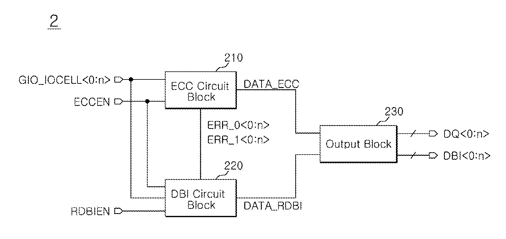
[0019]FIG. 1 is a configuration diagram illustrating examples of representations of a semiconductor memory apparatus in accordance with an embodiment.
[0020]The semiconductor memory apparatus 2 illustrated in FIG. 1 may include an error check and correction (ECC) circuit block 210 and a data bus inversion (DBI) circuit block 220. The semiconductor memory apparatus 2 may also include an output block 230.
[0021]During a read operation, the ECC circuit block 210 may receive a plurality of cell data GIO_IOCELL from a memory cell array through a global data transmission line. The ECC circuit block 210 may correct an error found the plurality of cell data GIO_IOCELL after receiving or in response to receiving an error check enable signal ECCEN. The ECC circuit block 210 may then output error-checked data DATA_ECC. Further, the ECC circuit block 210 m...
PUM
 Abstract
Description
Claims
Application Information