Organic electroluminescent element

Inactive Publication Date: 2015-08-13
IDEMITSU KOSAN CO LTD
View PDF5 Cites 5 Cited by
  • Summary
  • Abstract
  • Description
  • Claims
  • Application Information

AI Technical Summary

Benefits of technology

[0042]The organic EL device of the present invention is capable of bein

Problems solved by technology

In general, driving or storage of an organic EL device under a high temperature environment may cause such problems as change of the light emission color, deterioration of the light emission efficiency, increase of the driving voltage, reduction of the

Method used


Image

  • Organic electroluminescent element
  • Organic electroluminescent element
  • Organic electroluminescent element

Examples


example 1-1

Production of Organic EL Device

[0163]A glass substrate with ITO transparent electrode lines having a dimension of 25 mm×75 mm×1.1 mm in thickness (produced by Geomatec Co., Ltd.) was subjected to ultrasonic cleaning in isopropyl alcohol for 5 minutes and further subjected to UV (ultraviolet) ozone cleaning for 30 minutes.

[0164]The glass substrate with ITO transparent electrode lines thus cleaned was mounted on a substrate holder of a vacuum vapor deposition apparatus, and the electron accepting compound (A) shown below was vapor-deposited on the surface having the transparent electrode lines formed thereon to cover the transparent electrode, thereby forming a film A having a thickness of 5 nm. An aromatic amine derivative (X1) as a first hole transporting material shown below was vapor-deposited on the film A, thereby forming a first hole transporting layer having a thickness of 160 nm. Subsequent to the formation of the first hole transporting layer, an aromatic amine derivative (H...

examples 1-2 to 1-12

[0168]In Examples 1-2 to 1-12, organic EL devices were produced in the same manner as in Example 1-1 except that the following aromatic amine derivatives shown in Table 1 were used as the first hole transporting material and the second hole transporting material in Example 1-1.

example 2-1

Production of Organic EL Device

[0172]A glass substrate with ITO transparent electrode lines having a dimension of 25 mm×75 mm×1.1 mm in thickness (produced by Geomatec Co., Ltd.) was subjected to ultrasonic cleaning in isopropyl alcohol for 5 minutes and further subjected to UV (ultraviolet) ozone cleaning for 30 minutes.

[0173]The glass substrate with ITO transparent electrode lines thus cleaned was mounted on a substrate holder of a vacuum vapor deposition apparatus, and the electron accepting compound (A) shown below was vapor-deposited on the surface having the transparent electrode lines formed thereon to cover the transparent electrode, thereby forming a film A having a thickness of 5 nm. The aromatic amine derivative (X1) as a first hole transporting material was vapor-deposited on the film A, thereby forming a first hole transporting layer having a thickness of 65 nm. Subsequent to the formation of the first hole transporting layer, an aromatic amine derivative (H6) shown bel...


PUM

PropertyMeasurementUnit
Electric potential / voltageaaaaaaaaaa
Efficiencyaaaaaaaaaa

Abstract

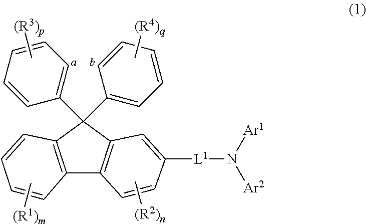
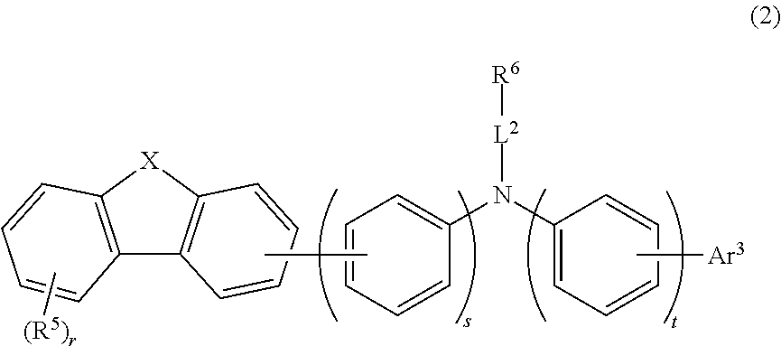
An organic electroluminescent device containing, between an anode and a cathode facing each other, a first hole transporting layer, an adjacent layer adjacent to an emitting layer, and an emitting layer, in this order from the side of the anode, wherein the first hole transporting layer contains a compound represented by the following formula (1), is provided as an organic EL device that is capable of being driven at a low voltage and has a prolonged life time and high efficiency. (In the formula, R1 to R4, L1, Ar1, Ar2, m, n, p and q are as defined in the specification.)

Description

TECHNICAL FIELD[0001]The present invention relates to an organic electroluminescent device. For example, the present invention relates to an organic electroluminescent device that uses an aromatic amine derivative having a substituted or unsubstituted 9,9-diphenylfluorene skeleton.BACKGROUND ART[0002]An organic electroluminescent (EL) device is generally constituted by an anode, a cathode, and at least one layer of an organic thin film layer that intervenes between the anode and the cathode. On applying a voltage between the electrodes, electrons and holes are injected from the side of the cathode and the side of the anode respectively to the light emitting region, and the electrons and the holes thus injected are recombined in the light emitting region to form an excited state, which then returns to the ground state to emit light. Accordingly, for providing an organic EL device having high efficiency, it is important to develop a compound that efficiently transports electrons and h...

Claims


Application Information

Patent Timeline
IPC IPC(8): H01L51/00C09K11/02
CPCH01L51/006H01L51/0061H01L51/0071H01L51/0072H01L51/0052H01L51/0094H01L51/0054H01L51/0055H01L51/0056H01L51/0067C09K11/02H01L51/5206C07D405/14C07C211/61C07D209/82C07D307/91C07C2603/18C09B57/008H10K85/633H10K85/6576H10K85/6574H10K85/6572H10K50/157H10K50/15H10K50/156H10K85/40H10K85/615H10K85/622H10K85/623H10K85/624H10K85/636H10K85/654H10K85/657H10K50/11H10K50/81H10K50/82H10K85/626H10K2102/00H10K2102/103
Inventor KATO, TOMOKISADO, TAKAYASU
Owner IDEMITSU KOSAN CO LTD
Why Eureka
Try Eureka