Cross-point memory and methods for fabrication of same

a technology of cross-point memory and fabrication methods, which is applied in the direction of bulk negative resistance effect devices, semiconductor devices, electrical equipment, etc., can solve the problems of damaging and contaminating the sidewalls of the stacked structure being etched, and unsatisfactory effects

Active Publication Date: 2015-08-27
MICRON TECH INC
View PDF9 Cites 126 Cited by
  • Summary
  • Abstract
  • Description
  • Claims
  • Application Information

AI Technical Summary

Problems solved by technology

Patterning the memory elements, which often involve etching at least portions of a stack of materials to form a stacked structure, for exam

Method used


Image

  • Cross-point memory and methods for fabrication of same
  • Cross-point memory and methods for fabrication of same
  • Cross-point memory and methods for fabrication of same

Examples


Embodiment Construction

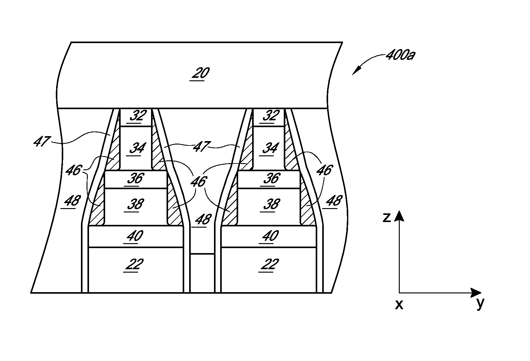
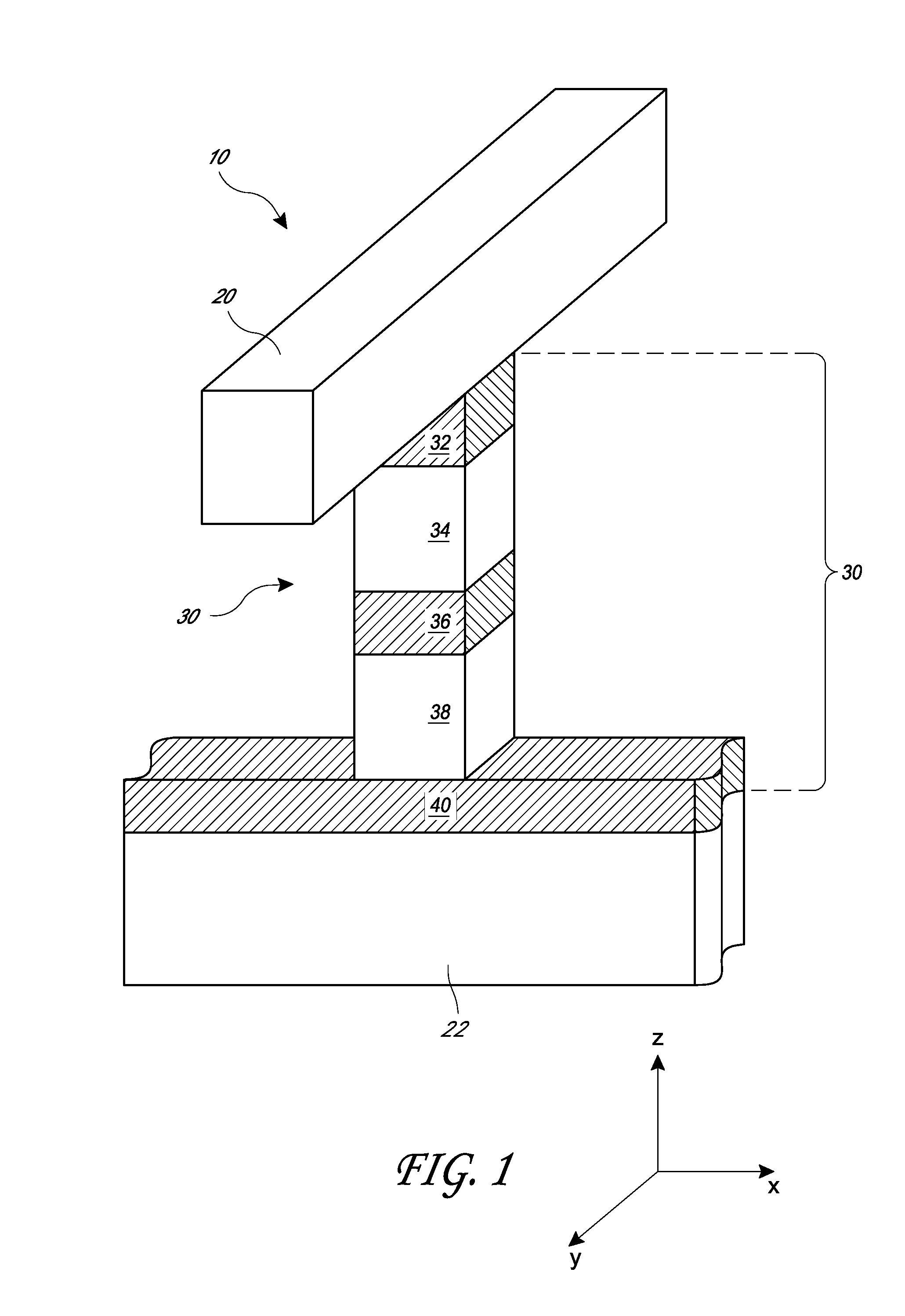
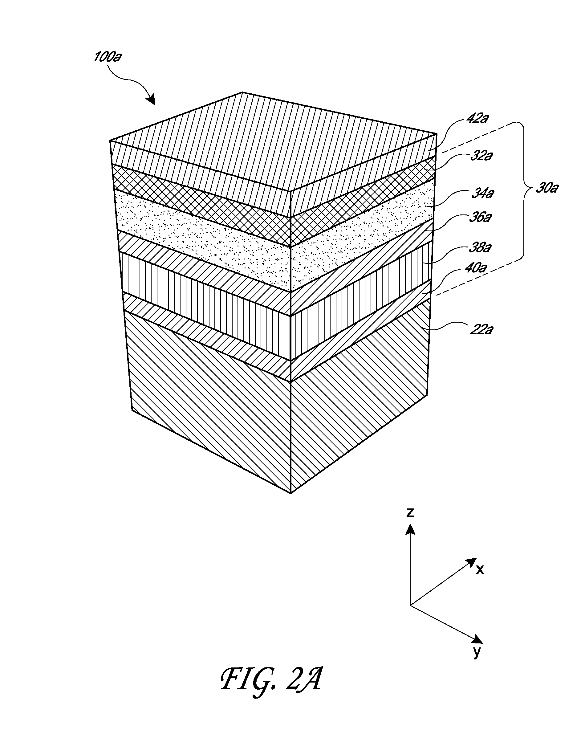
[0014]As noted above, generally, a cross-point memory array refers to a memory array having memory cells disposed and electrically connected at cross-junctions between a first set of conductive lines (e.g., word lines) and a second set of conductive lines (e.g., bit lines) overlapping and crossing the first set of conductive lines. The memory cells can change their memory state in response to a signal, which can be an electrical signal such as a voltage or a current pulse. Some memory cells, sometimes called the resistance change cells, incorporate resistance change materials whose electrical resistance can be changed by the electrical signals provided through the first and second conductive lines connected to the resistance change materials. One category of such resistance change materials is that of phase change materials, such as but not limited to chalcogenide materials.

[0015]The memory cells in a cross-point memory array can include multiple elements arranged in a stacked confi...


PUM


Abstract

The disclosed technology relates generally to integrated circuit devices, and in particular to cross-point memory arrays and methods for fabricating the same. In one aspect, a method of fabricating cross-point memory arrays comprises forming a memory cell material stack which includes a first active material and a second active material over the first active material, wherein one of the first and second active materials comprises a storage material and the other of the first and second active materials comprises a selector material. The method of fabricating cross-point arrays further comprises patterning the memory cell material stack, which includes etching through at least one of the first and second active materials of the memory cell material stack, forming protective liners on sidewalls of the at least one of the first and second active materials after etching through the one of the first and second active materials, and further etching the memory cell material stack after forming the protective liners on the sidewalls of the one of the first and second active materials.

Description

REFERENCE TO RELATED APPLICATIONS[0001]This application is related to application Ser. No. ______filed on even date herewith, attorney docket no. MICRON.638A [Micron ref. 2013-0325], entitled CROSS-POINT MEMORY AND METHODS FOR FABRICATION OF SAME; application Ser. No. ______, filed on even date herewith, attorney docket no. 2269-12097US [Micron ref. 2013-0465], entitled SEMICONDUCTOR STRUCTURES INCLUDING LINERS COMPRISING ALUCONE AND RELATED METHODS, filed on even date herewith.BACKGROUND OF THE INVENTION[0002]1. Field of the Invention[0003]Subject matter disclosed herein generally relates to integrated circuit devices, and in particular to cross-point memory arrays and methods for fabricating the same.[0004]2. Description of the Related Art[0005]Generally, a cross-point memory array refers to a memory array having memory elements disposed and electrically connected at cross-junctions between a first set of conductive lines (e.g., word lines) and a second set of conductive lines (e....

Claims


Application Information

Patent Timeline
IPC IPC(8): H01L27/24H01L45/00
CPCH01L27/2463H01L45/06H01L45/1233H01L45/141H01L45/1608H01L45/1675H01L45/1253H10B63/24H10B63/80H10N70/801H10N70/231H10N70/20H10N70/826H10N70/8828H10N70/8833H10N70/063H10N70/011
Inventor RAVASIO, MARCELLOSCIARRILLO, SAMUELEPELLIZZER, FABIOTORTORELLI, INNOCENZOSOMASCHINI, ROBERTOCASELLATO, CRISTINAMOTTADELLI, RICCARDO
Owner MICRON TECH INC
Why Eureka
Try Eureka