Multi-layer expanding electrode structures for backplane assemblies

a backplane assembly and electrode structure technology, applied in the direction of semiconductor devices, semiconductor/solid-state device details, instruments, etc., can solve the problems of preventing widespread use of these displays, inadequate service life of these displays, and gas-based electrophoretic media being susceptible to the same types of problems

Active Publication Date: 2015-09-17
E INK CORPORATION
View PDF4 Cites 76 Cited by
  • Summary
  • Abstract
  • Description
  • Claims
  • Application Information

AI Technical Summary

Problems solved by technology

Nevertheless, problems with the long-term image quality of these displays have prevented their widespread usage.
For example, particles that make up electrophoretic displays tend to settle, resulting in inadequate service-life for these displays.
Such gas-based electrophoretic media appear to be susceptible to the same types of problems due to particle settling as liquid-based electrophoretic media, when the media are used in an orientation which permits such settling, for example in a sign where the medium is disposed in a vertical plane.
Indeed, particle settling appears to be a more serious problem in gas-based electrophoretic media than in liquid-based ones, since the lower viscosity of gaseous suspending fluids as compared with liquid ones allows more rapid settling of the electrophoretic particles.
However, the methods used for assembling LCD's cannot be used with encapsulated electrophoretic displays.
This LCD assembly process cannot readily be transferred to encapsulated displays.
Electro-optic displays, including electrophoretic displays, can be costly; for example, the cost of the color LCD found in a portable computer is typically a substantial fraction of the entire cost of the computer.
Such large area displays are frequently formed by “tiling” (i.e., juxtaposing) a two-dimensional array of discrete electro-optic displays together since, for technical reasons, such as limitations on the size of backplane assemblies produced by photolithography, individual electro-optic displays cannot economically exceed a certain size.
Unfortunately, conventional electro-optic displays require driver electronics which are normally disposed around the periphery of the display.
However, such peripheral driver electronics do create a problem when multiple displays are used to form a large area display since the peripheral areas are inherently optically inactive.

Method used


Image

  • Multi-layer expanding electrode structures for backplane assemblies
  • Multi-layer expanding electrode structures for backplane assemblies
  • Multi-layer expanding electrode structures for backplane assemblies

Examples


Embodiment Construction

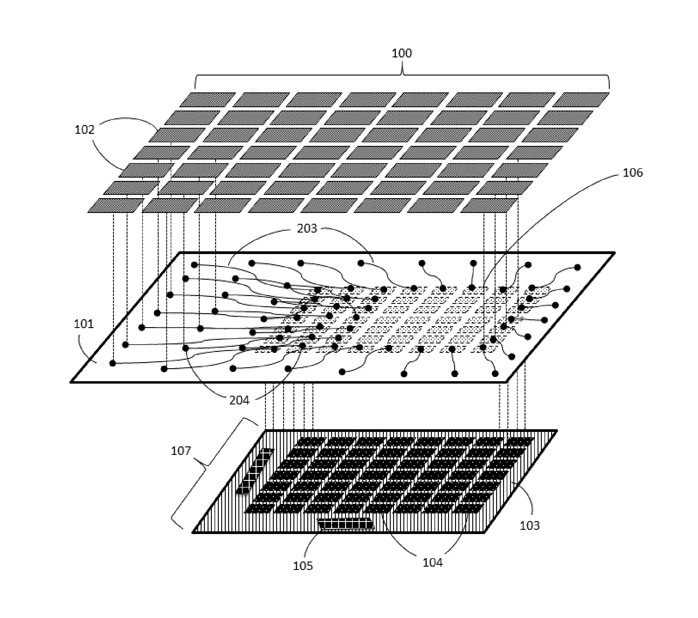
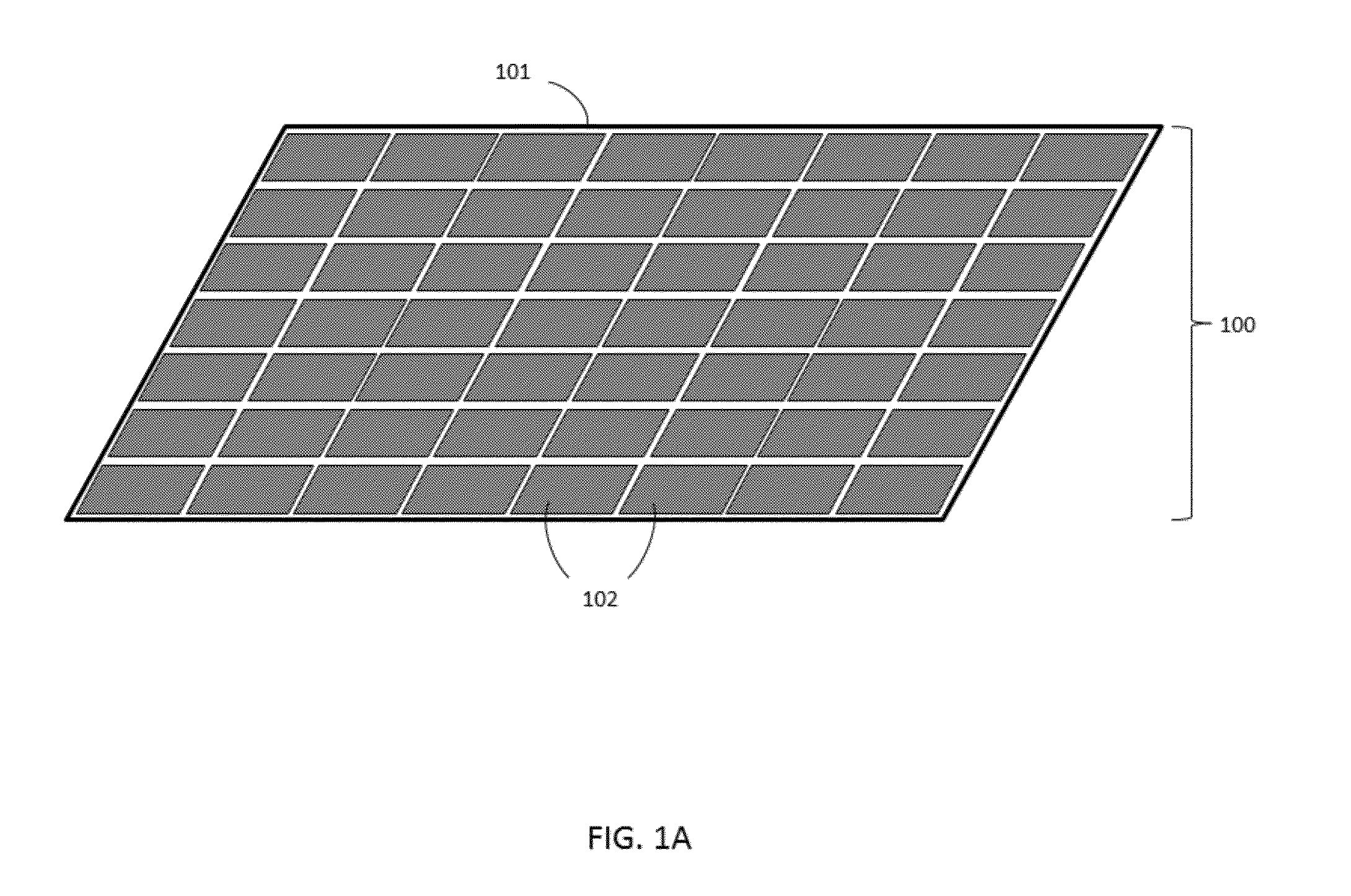
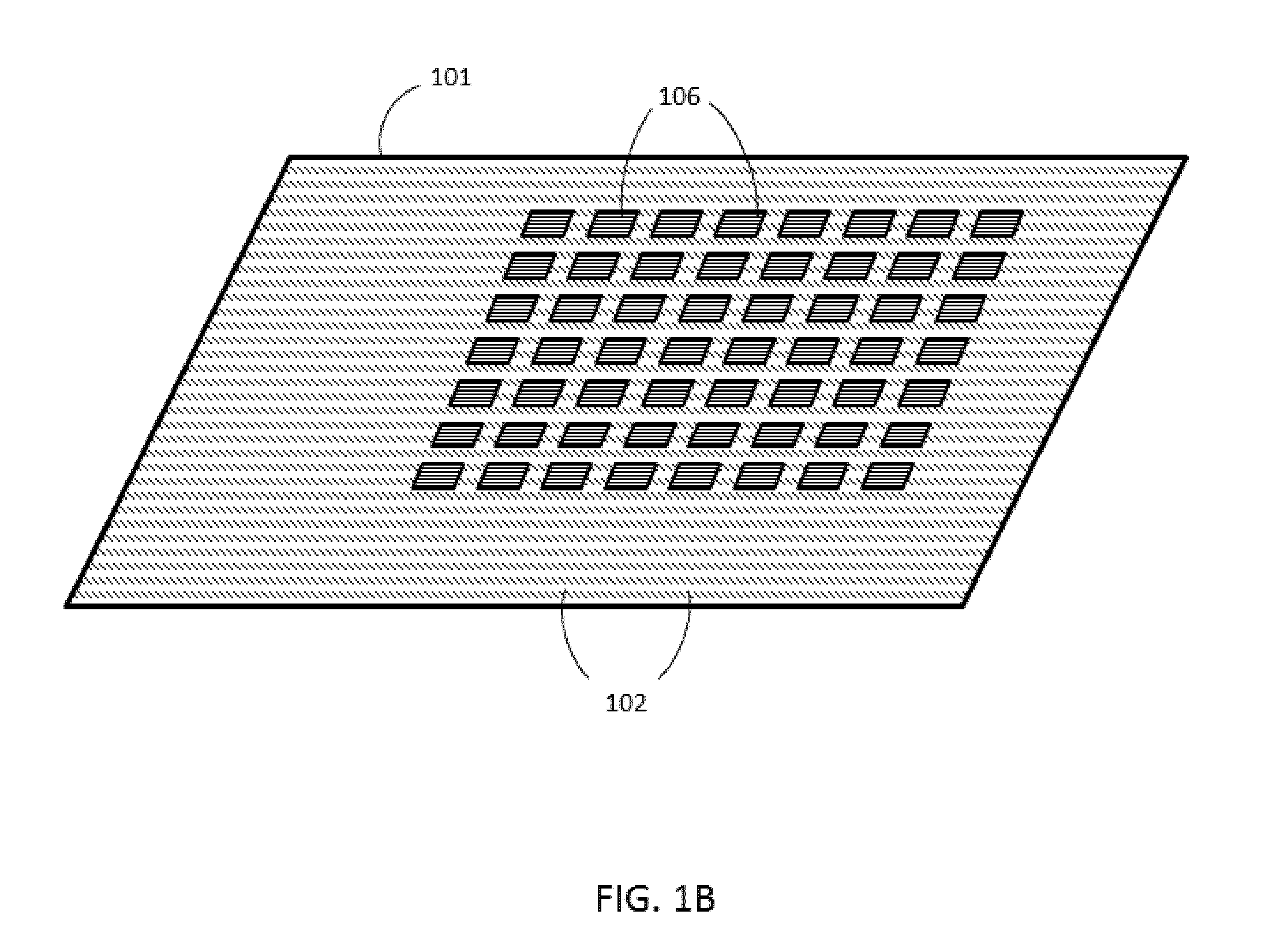
[0047]As indicated above, the present invention provides for an electro-optic display having a backplane assembly with at least two electrode layers and at least one interposer layer disposed between the two electrode layers, a first electrode layer of a first dimension electrically connected to and driving a second electrode layer of a second dimension that is larger than the first dimension, such that the viewing surface may be completely optically-active.

[0048]In another aspect, the present invention provides for an electro-optic display having a backplane assembly with at least three electrode layers and at least one interposer layer disposed between the second and third electrode layers, a first electrode layer electrically connected to a third electrode layer, a third electrode layer electrically connected through an interposer layer to a second electrode layer, wherein the first electrode layer dimension is smaller than the second electrode layer dimension and wherein the fir...


PUM

PropertyMeasurementUnit
sizeaaaaaaaaaa
sizeaaaaaaaaaa
diameteraaaaaaaaaa

Abstract

The present invention provides for an electro-optic display having a backplane assembly with at least two electrode layers, a first electrode layer of a first dimension electrically connected to and driving a second electrode layer of a second dimension that is larger than the first dimension. The second electrode layer overlies the first electrode layer, such that the entire viewing area of an electro-optic display may be optically-active. The backplane assembly may have at least one interposer layer disposed between the two electrode layers to electrically connect the first and second electrode layers.

Description

REFERENCE TO RELATED APPLICATIONS[0001]This application is related to copending U.S. application Ser. No. 14 / 615,617, filed on Feb. 6, 2015.[0002]The entire contents of these copending applications, and of all other U.S. patents and published and copending applications mentioned below, are herein incorporated by reference.BACKGROUND OF INVENTION[0003]In applications where individual electro-optic displays are tiled together to create a larger display, it is optimal for the viewing area to be completely active. Accordingly, the present invention provides for an electro-optic display having a backplane assembly with at least two electrode layers and at least one interposer layer disposed between the two electrode layers, a first electrode layer of a first dimension electrically connected to and driving a second electrode layer of a second dimension that is larger than the first dimension, such that the entire viewing surface area of the second electrode layer may be optically-active.[...

Claims


Application Information

Patent Timeline
Patent Type & Authority Applications(United States)
IPC IPC(8): G02F1/167H01L27/12G02F1/163G02B26/02G02B26/00G02F1/16766
CPCG02F1/167G02B26/026G02B26/005G02F2001/1635H01L27/124G02F2001/1676G02F1/163G02F1/13336G02F1/13452G02F2201/12G02F2201/42G02F1/16766
Inventor HARRIS, GEORGE G.TELFER, STEPHEN J.PAOLINI, JR., RICHARD J.
Owner E INK CORPORATION
Why Eureka
Try Eureka