Packaging film for display device

a display device and packaging film technology, applied in the direction of packaging goods, instruments, transportation and packaging, etc., can solve the problems of reducing sealability, light leakage phenomenon, and affecting the appearance of the display device according to the conventional art, and achieve the effect of minimizing the bezel region

Inactive Publication Date: 2015-09-24
LG CHEM LTD
View PDF6 Cites 5 Cited by
  • Summary
  • Abstract
  • Description
  • Claims
  • Application Information

AI Technical Summary

Benefits of technology

[0014]The present application is directed to providing a packaging film for a display device through which an improved display device can be embodied. The present application provides, for example, a packaging film for a display device that minimizes a bezel region.

Problems solved by technology

In addition, the display device according to the conventional art may have problems in handling and assembly of the backward diode, that is, the backlight unit 20.
Moreover, according to the assembly using the molding frame 30, a light leakage phenomenon may occur due to decreased sealability.
Such a problem may bring an increase in costs and a decrease in yield of the display device, and have a bad influence on performance.

Method used


Image

  • Packaging film for display device
  • Packaging film for display device
  • Packaging film for display device

Examples


first embodiment

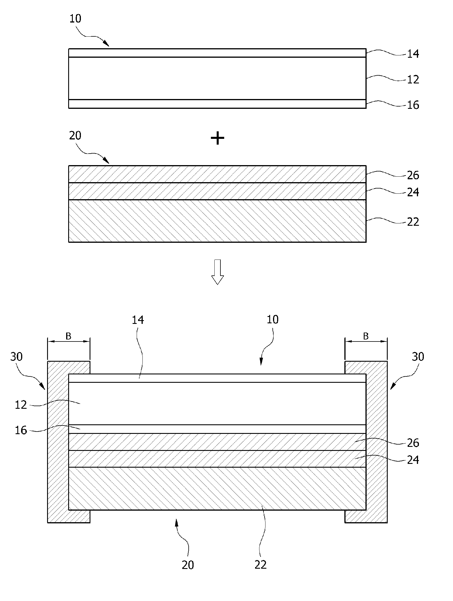
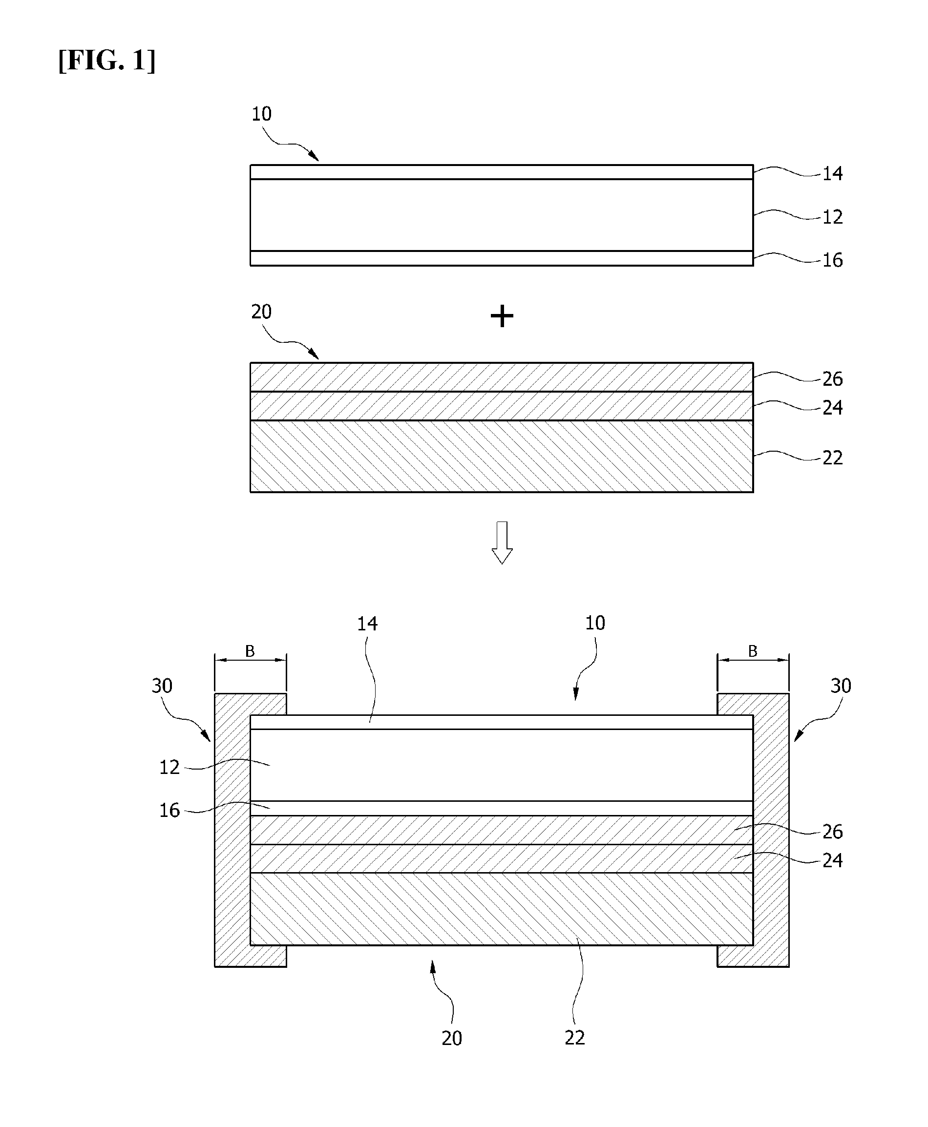
[0063]Examples of the packaging film 300 according to the first embodiment of the present application are shown in FIGS. 2 to 9.

[0064]The packaging film 300 according to the first embodiment of the present application packages a backward diode 200 equipped on a bottom surface of a display panel 100. The packaging film 300 surrounds and packages at least a top surface 201 and a side surface 202 of the backward diode 200. To this end, the packaging film 300 includes a first region 310 corresponding to the top surface 201 of the backward diode 200 and a second region 320 corresponding to the side surface 202 of the backward diode 200. The second region 320 extends from the first region 310.

[0065]The display device includes the packaging film 300 described in the present application. According to an exemplary embodiment, the display device includes a display panel 100, a backward diode 200 equipped on a bottom surface of the display panel 100, a packaging film 300 for packaging the back...

second embodiment

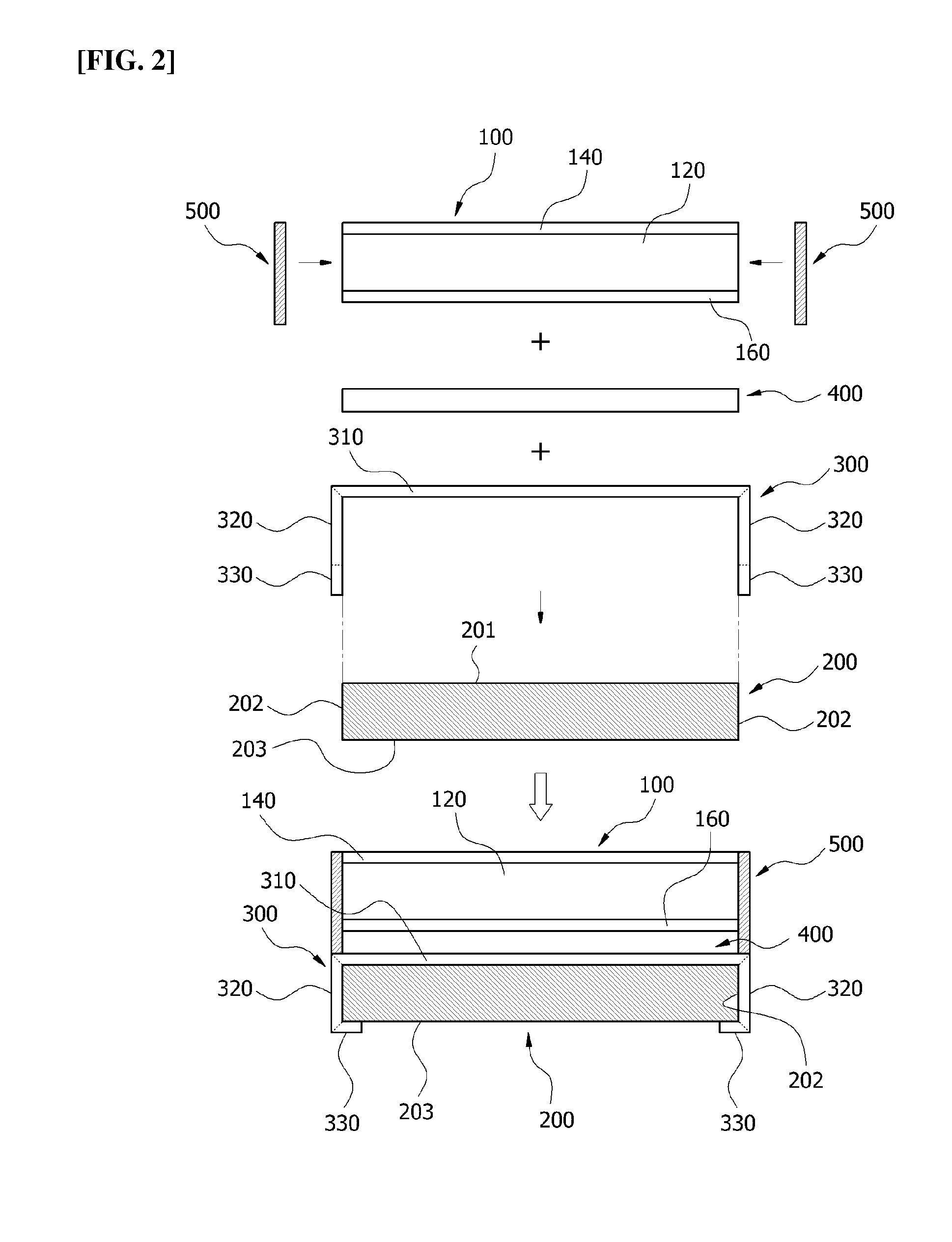
[0230]Hereinafter, a packaging film 300′ according to a second embodiment of the present application will be explained.

[0231]In FIGS. 10 to 17, examples of the packaging film 300′ according to the second embodiment of the present application are shown. To explain the second embodiment of the present application, the same terms and reference marks as in the first embodiment exhibit the same functions, and thus detailed description thereof will be omitted. Hereinafter, any part that is not specifically explained is the same as in the first embodiment. For example, this applies to materials and physical properties of the packaging film 300′. In addition, in some cases, the first embodiment may include a configuration of the second embodiment which will be explained below.

[0232]The packaging film 300′ surrounds and packages a top surface 101 and a side surface 102 of a display panel 100. In addition, the packaging film 300′ surrounds and packages at least a side surface 202 of a backwar...


PUM

PropertyMeasurementUnit
thickness-direction retardationaaaaaaaaaa
temperature storage modulusaaaaaaaaaa

Abstract

Provided is a packaging film for a display device, which includes a first region corresponding to a top surface of a backward diode equipped on a bottom surface of a display panel; and a second region extending from the first region and corresponding to a side surface of the backward diode. Due to the packaging film, a bezel region can be minimized.

Description

BACKGROUND[0001]1. Field of the Invention[0002]The present application relates to a packaging film for a display device with which an improved display device can be embodied.[0003]2. Discussion of Related Art[0004]A display device is useful in various electronic products. For example, a device such as a liquid crystal display (LCD) is used in various products including a mobile phone, a personal digital assistant (PDA), an electronic game console, a monitor and a TV.[0005]Generally, a display device has a display panel displaying an image. In addition, most of the display devices include a backward diode equipped on a bottom surface of the display panel. For example, an LCD device includes a back light unit (BLU) as a backward diode.[0006]FIG. 1 is a cross-sectional diagram showing a display device, and particularly, an LCD device, according to conventional art.[0007]Referring to FIG. 1, the LCD device has an LCD panel 10 displaying an image. Generally, the LCD panel 10 is not self-...

Claims


Application Information

Patent Timeline
Patent Type & Authority Applications(United States)
IPC IPC(8): G02F1/1333B65D65/14B65D85/38B65D65/38
CPCG02F1/1333B65D85/38B65D65/14B65D65/38G02F1/133308G02F1/133325G02B6/0088G02B6/0051Y10T428/2419G02F1/133314
Inventor YANG, SE WOOSEO, KUM SUEKPARK, JONG SUNGPARK, MIN SOOHWANG, JI YOUNGJUNG, JAE HOMUN, IN JUPARK, YONG SU
Owner LG CHEM LTD
Why Eureka
Try Eureka