Grid and nanostructure transparent conductor for low sheet resistance applications

a transparent conductor, nanostructure technology, applied in the direction of conductive pattern formation, instruments, synthetic resin layered products, etc., can solve the problems of adverse affecting other physical (transmission properties, time, flexibility, etc., to reduce the overall cost of materials, reduce the surface roughness, and reduce the effect of leakage curren

Active Publication Date: 2015-10-29
CHAMP GREAT INTL
View PDF2 Cites 0 Cited by
  • Summary
  • Abstract
  • Description
  • Claims
  • Application Information

AI Technical Summary

Benefits of technology

[0009]An example transparent conductor method is described herein. A low sheet resistance grid is deposited on a planar transfer film surface according to a grid pattern. A nanostructure layer is also deposited on the transfer film surface according to a nanostructure layer pattern. The low sheet resistance grid and the nanostructure layer form a coplanar transparent conductor surface. The resultant transparent conductor has high transparency, low sheet resistance, and minimal surface roughness.
[0010]An example transparent conductor is also described herein. The transparent conductor includes a low sheet resistance grid and a nanostructure layer forming a transparent conductor having a coplanar surface. The resultant transparent conductor has high transparency, low sheet resistance, and minimal surface roughness.

Problems solved by technology

However, transparent conductors such as Indium-Tin Oxide (ITO) and Aluminum doped Zinc Oxide (AZO) have practical limitations in the lowest economically or practically obtainable sheet resistance.
Where low sheet resistance ITO or AZO based thermal conductors are needed, other physical (transmission properties, deposition time, flexibility) or fiscal (processing time, overall cost of materials) properties are adversely impacted.
In addition to opacity concerns with high conductor density grids, many composite metal grid transparent conductors have an inherently three dimensional surface, the presence of which can result in compromised performance of electronic devices using such transparent conductor through excessive leakage current or shorting.

Method used


Image

  • Grid and nanostructure transparent conductor for low sheet resistance applications
  • Grid and nanostructure transparent conductor for low sheet resistance applications
  • Grid and nanostructure transparent conductor for low sheet resistance applications

Examples


Embodiment Construction

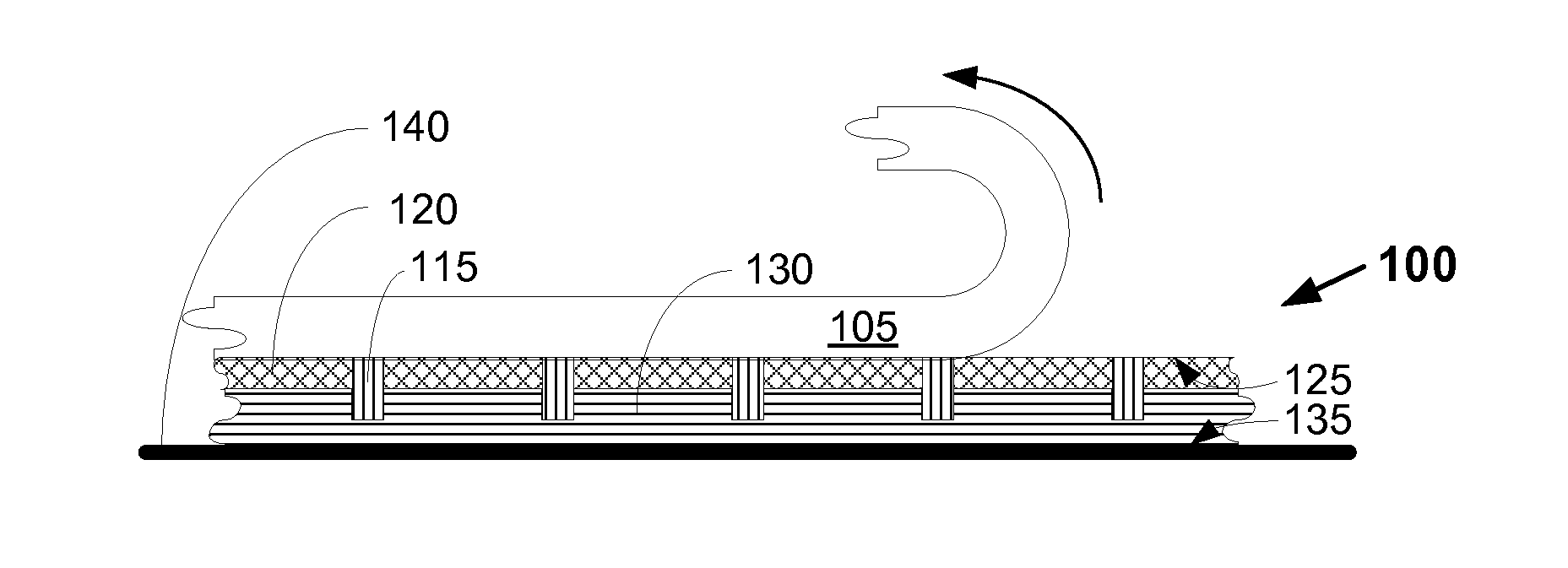
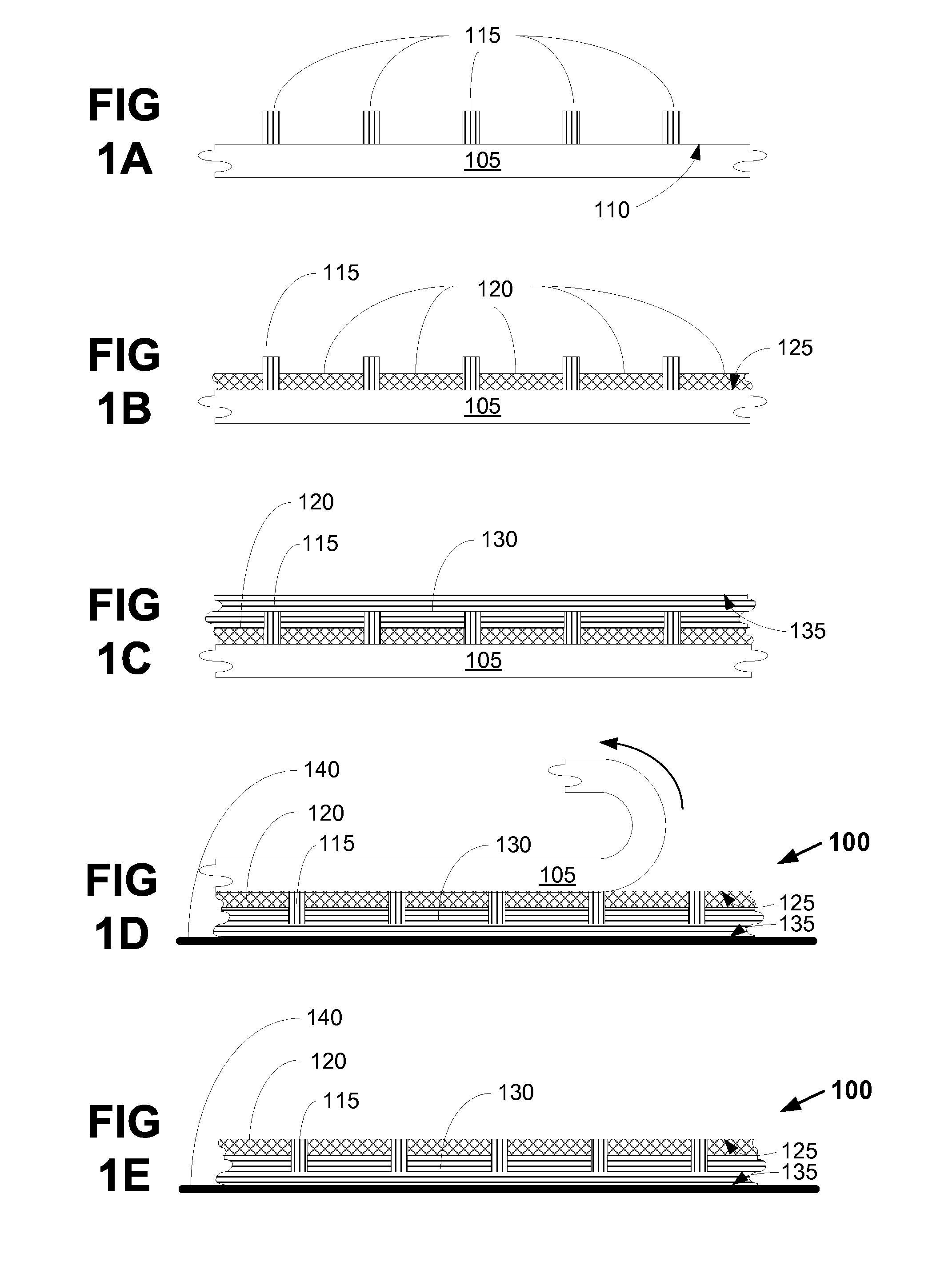
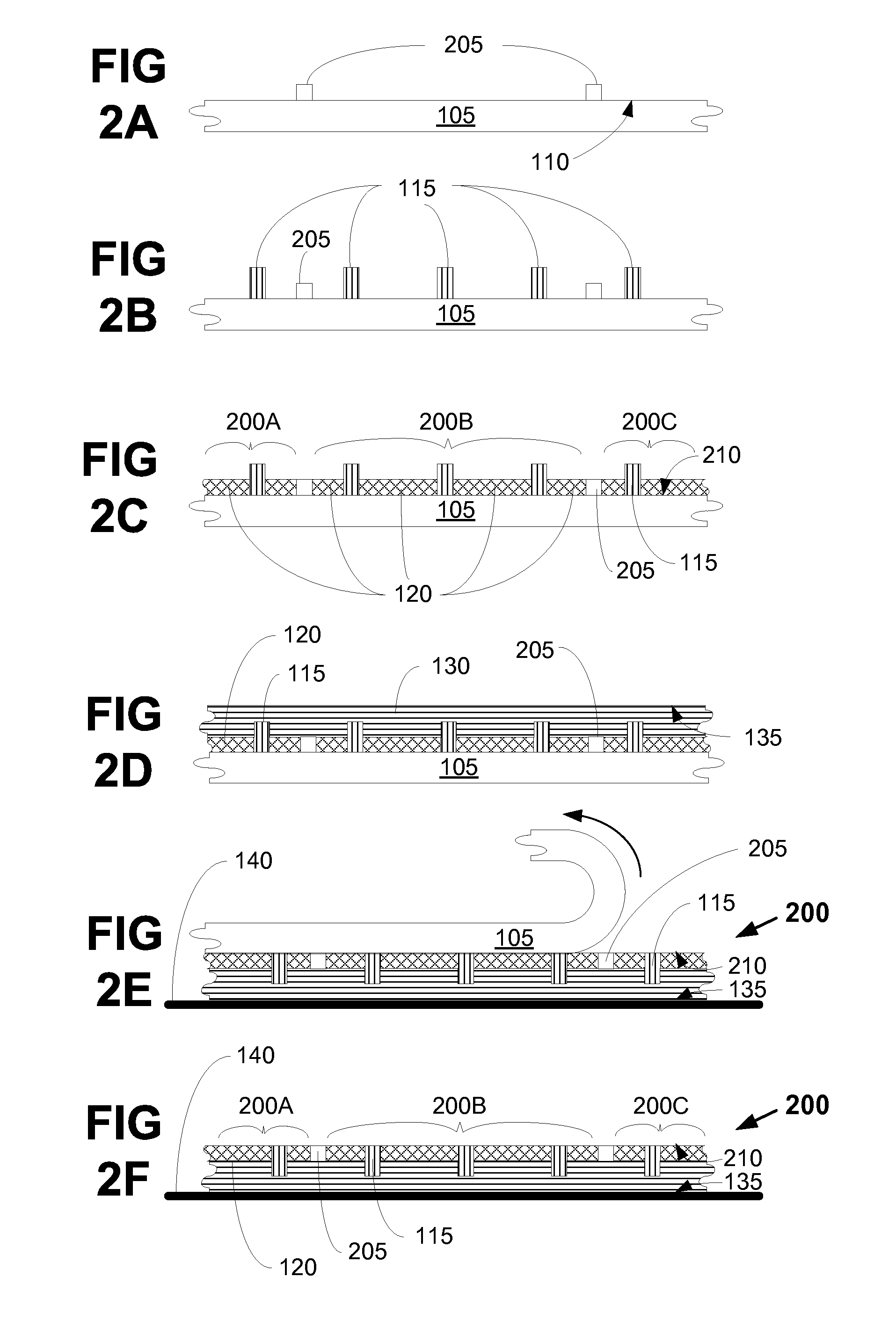
[0018]The transparent conductors and transparent conductor methods described herein are presented in the form of various embodiments. It should be understood that variations are possible within each of these embodiments and in other embodiments not specifically described for the sake of clarity and / or to avoid redundancy within this disclosure. Additionally, the order and extent of deposition of the various layers and structures disclosed herein can be varied, altered, divided, or subdivided to meet varying performance specifications. The general format presented will provide, in making reference to all included illustrated embodiments in FIGS. 1-6, a detailed description of each of the components used within the illustrative embodiments provided herein. A detailed description of each illustrated embodiment follows the detailed component descriptions.

[0019]The various layers discussed may comprise one or more independently applied layers. Different layers may be applied uniformly (e...


PUM

PropertyMeasurementUnit
surface roughnessaaaaaaaaaa
sheet resistancesaaaaaaaaaa

Abstract

Transparent conductors and methods of forming same are provided. A transparent conductor can include a nanostructure layer and a low sheet resistance grid disposed on a transfer film surface having an acceptable level of surface roughness. The presence of the low sheet resistance grid lowers the sheet resistance of the transparent conductor to an acceptable level. After release of the transparent conductor from the transfer film, the surface roughness of the transparent conductor will be at least comparable to the surface roughness of the transfer film.

Description

CROSS-REFERENCE TO RELATED APPLICATIONS[0001]This application is a divisional of U.S. application Ser. No. 13 / 287,881, having a filing date of Nov. 2, 2011, now pending, which claims the benefit of U.S. Provisional Patent Application No. 61 / 409,412 filed Nov. 2, 2010, both of which are incorporated herein by reference in their entirety.BACKGROUND[0002]1. Technical Field[0003]This invention is related to transparent conductors, in particular to transparent conductors having high transparency, low sheet resistance and low surface roughness.[0004]2. Description of the Related Art[0005]Transparent conductors refer to thin conductive films coated on high-transmittance insulating surfaces or substrates. Transparent conductors may be manufactured to have surface conductivity while maintaining reasonable optical transparency. Such surface conducting transparent conductors are widely used as transparent electrodes in flat liquid crystal displays, touch panels, electroluminescent devices, and...

Claims


Application Information

Patent Timeline
Patent Type & Authority Applications(United States)
IPC IPC(8): H05K3/10B05D5/00
CPCB05D5/00H05K3/10Y10T156/10G06F2203/04103H10K71/60H10K71/80H10K50/816H10K59/1201
Inventor GUPTA, RAHULPSCHENITZKA, FLORIANPICHLER, KARL
Owner CHAMP GREAT INTL
Why Eureka
Try Eureka