Wideband transition between a planar transmission line and a waveguide

Inactive Publication Date: 2015-12-10
NEC CORP
View PDF2 Cites 35 Cited by
  • Summary
  • Abstract
  • Description
  • Claims
  • Application Information

AI Technical Summary

Problems solved by technology

It is a crucial problem providing transmittance of an electromagnetic wave between a microwave circuit element and an antenna with low re

Method used


Image

  • Wideband transition between a planar transmission line and a waveguide
  • Wideband transition between a planar transmission line and a waveguide
  • Wideband transition between a planar transmission line and a waveguide

Examples


Embodiment Construction

[0059]Hereinafter, several types of wideband transitions disposed in multilayer substrates between a planar transmission line and a waveguide according to the present invention will be described in details with reference to attached drawings. But, it would be well understood that this description should not be viewed as narrowing the appended claims.

An Exemplary Embodiment

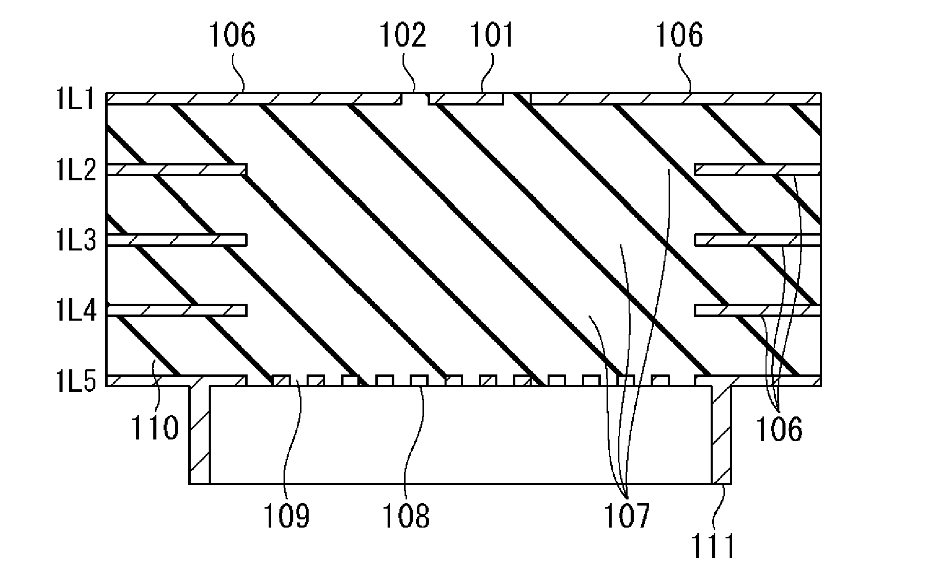
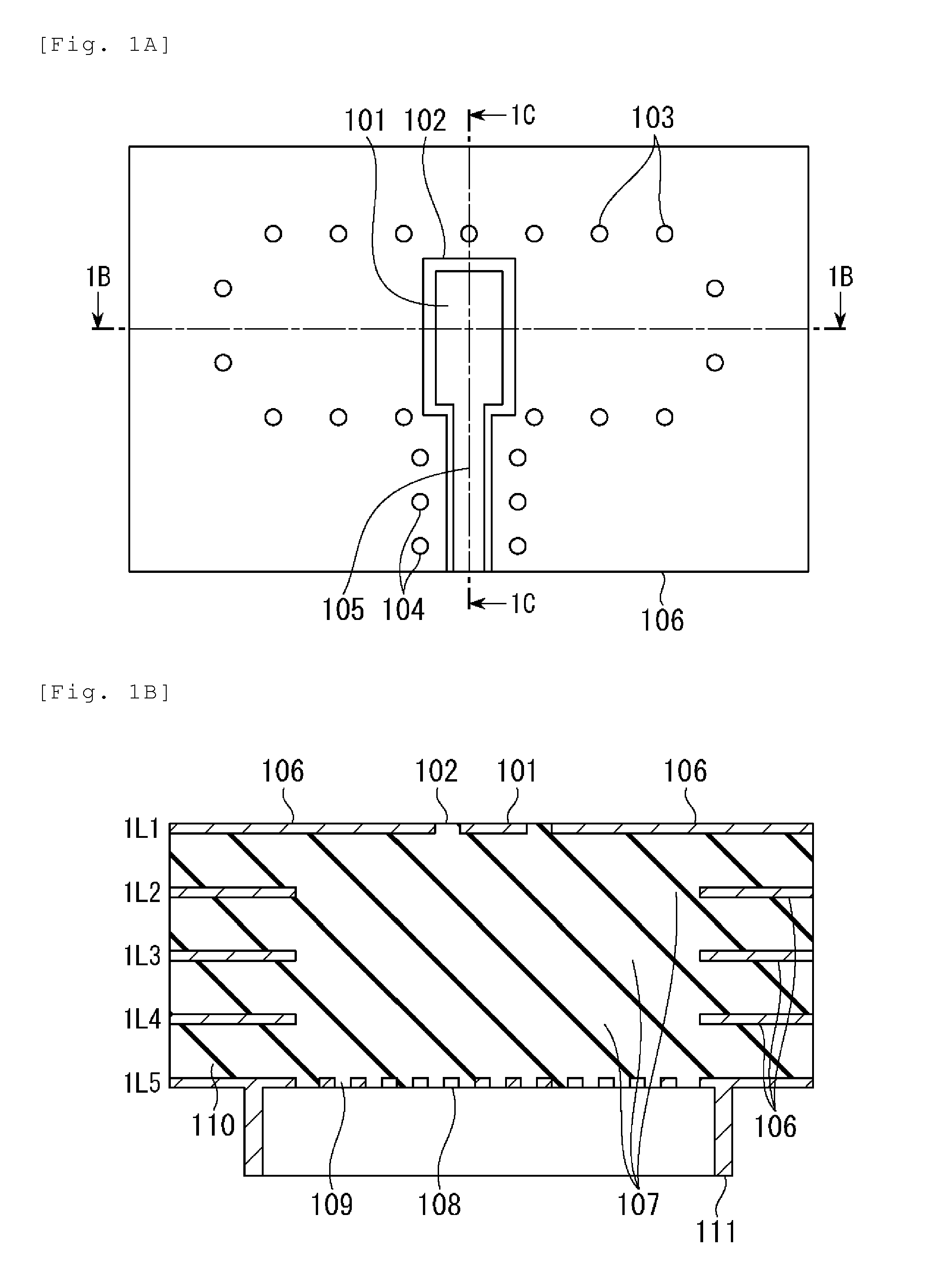
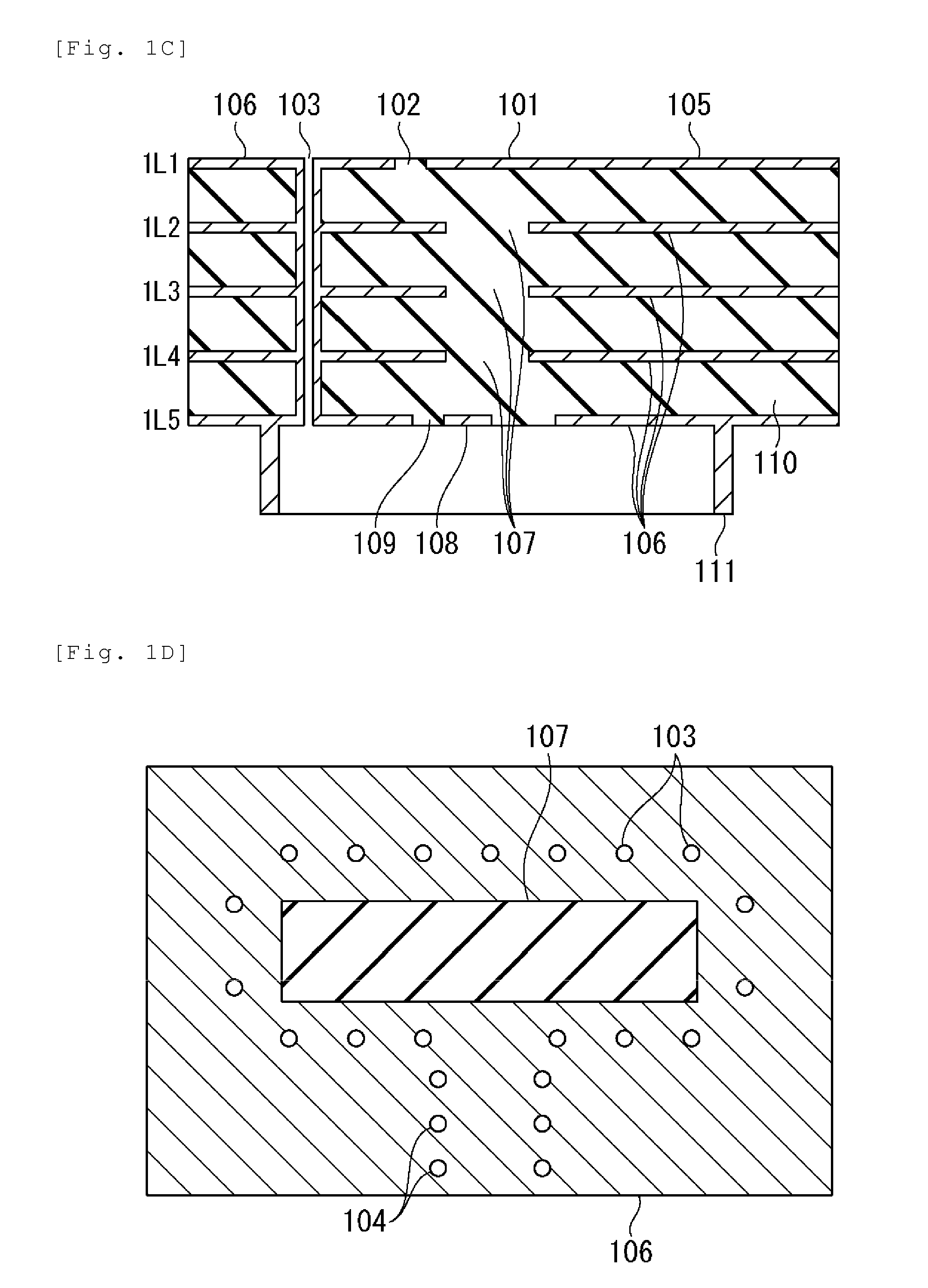
[0060]FIG. 1A is a top view of a wideband transition between a planar transmission line and a waveguide of an exemplary embodiment of the present invention. FIG. 1A shows a conductive patch 101, an isolating slit 102, a plurality of ground vias 103 of the wideband transition, a segment of a planar transmission line 105 and a plurality of ground vias 104 of the planar transmission line 105. FIG. 1A also shows two section lines 1B-1B and 1C-1C.

[0061]FIG. 1B is a vertical cross-sectional view of the wideband transition shown in FIG. 1A on 1B-1B section. FIG. 1B shows the conductive patch 101, the isolating slit 102, a...


PUM


Abstract

A wideband transition between a planar transmission line and a waveguide of this invention comprises a substrate, a segment of the planar transmission line and a section of the waveguide. The substrate includes a plurality of conductor-layers stacked from top to bottom and isolated by an insulating material. The segment of the planar transmission line is disposed in a top conductor-layer of the plurality of conductor-layers. The section of the waveguide is disposed on a bottom conductor-layer of the plurality of conductor-layers by a first end. The substrate comprises a conductive patch and a conductive dispersion plate. The conductive patch is disposed in the top conductor-layer and connected to a first end of said segment. The conductive dispersion plate is disposed in the bottom conductor-layer and under the conductive patch. The conductive dispersion plate comprises a corrugation.

Description

TECHNICAL FIELD[0001]The present invention relates to a wideband transition between a microwave circuit and an antenna.BACKGROUND ART[0002]It is a crucial problem providing transmittance of an electromagnetic wave between a microwave circuit element and an antenna with low return and insertion losses in a microwave (millimeter-wave) module in different practical applications, including automotive radar systems. An appropriate transition structure can improve energy consumption in the systems.[0003]In inventions U.S. Pat. No. 5,867,073, U.S. Pat. No. 6,127,901, US 2008 / 0129408 and US 2012 / 0050125, different structures of the transition between a planar transmission line and a waveguide are proposed.[0004]However, development of the transition operating in a wide frequency band is vital for providing a low-cost microwave (millimeter-wave) module overcoming fabrication process tolerance problems.CITATION LISTPatent Literature[0005][PTL 1] U.S. Pat. No. 5,867,073[0006][PLT 2] U.S. Pat. ...

Claims


Application Information

Patent Timeline
IPC IPC(8): H01P5/08H01P3/08
CPCH01P5/08H01P3/082H01P3/088H01P5/107
Inventor KUSHTA, TARAS
Owner NEC CORP
Why Eureka
Try Eureka