Flexible printed circuit board and manufacturing method of flexible printed circuit board

a manufacturing method and printed circuit board technology, applied in the direction of dielectric characteristics, printed element electric connection formation, waveguides, etc., can solve the problems of bending or disconnection of cables, reducing functions (operation speed, accuracy and the like), and increasing manufacturing costs

Active Publication Date: 2016-01-21
NIPPON MEKTRON LTD
View PDF3 Cites 54 Cited by
  • Summary
  • Abstract
  • Description
  • Claims
  • Application Information

AI Technical Summary

Benefits of technology

[0022]The present invention can create a state where a disconnection does not easily occur in a flexible printed circuit board even

Problems solved by technology

When such cables and hoses are arranged in a joint part, there is a chance that bending or disconnection of the cables occurs.
However, in the method of arranging the cables in the outside space of the robot arm, it becomes required to provide the space for slackening the cables to the periphery of the joint part of the robot arm.
However, there is a chance of causing a reduction in functions (operating speed, accuracy and the like) due to an increase in weight caused by separately providing the support rod.
There is sometimes a case

Method used


Image

  • Flexible printed circuit board and manufacturing method of flexible printed circuit board
  • Flexible printed circuit board and manufacturing method of flexible printed circuit board
  • Flexible printed circuit board and manufacturing method of flexible printed circuit board

Examples


first configuration example

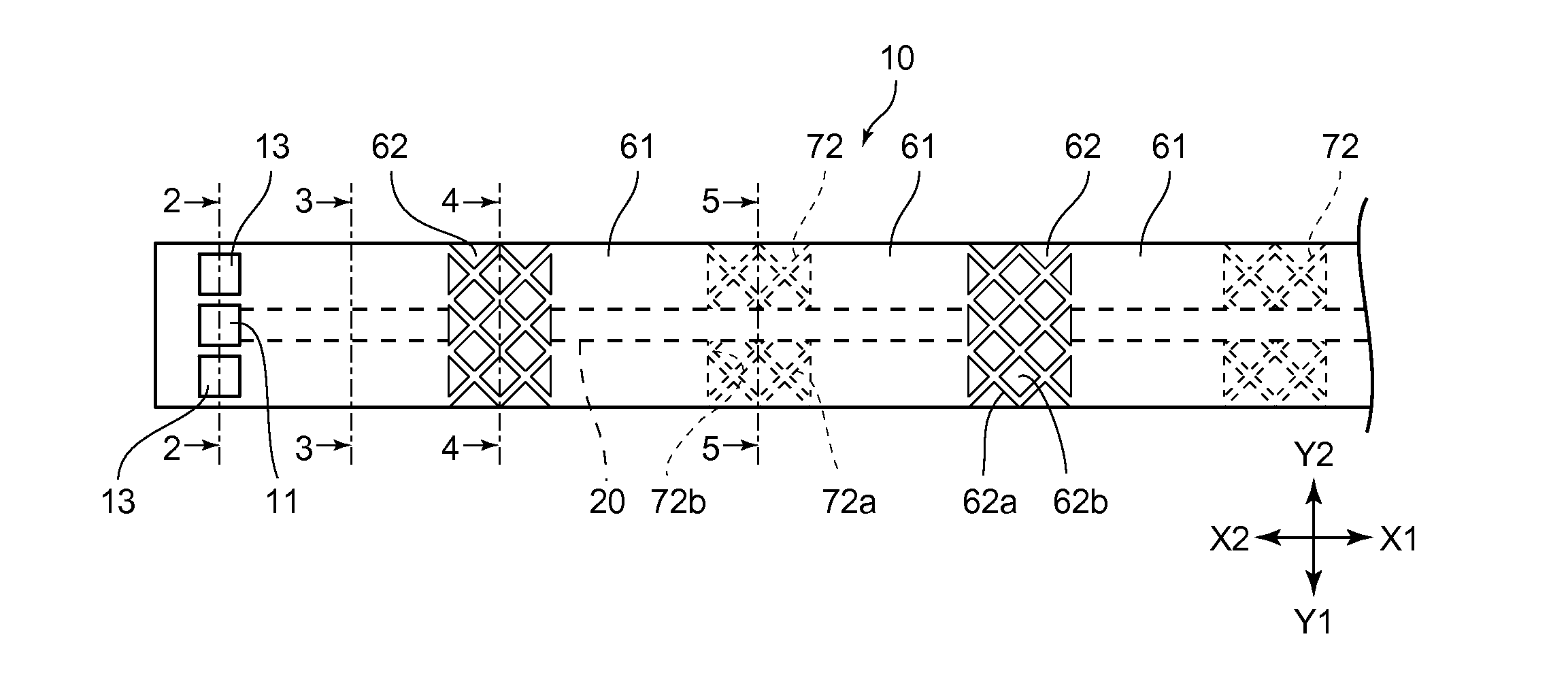
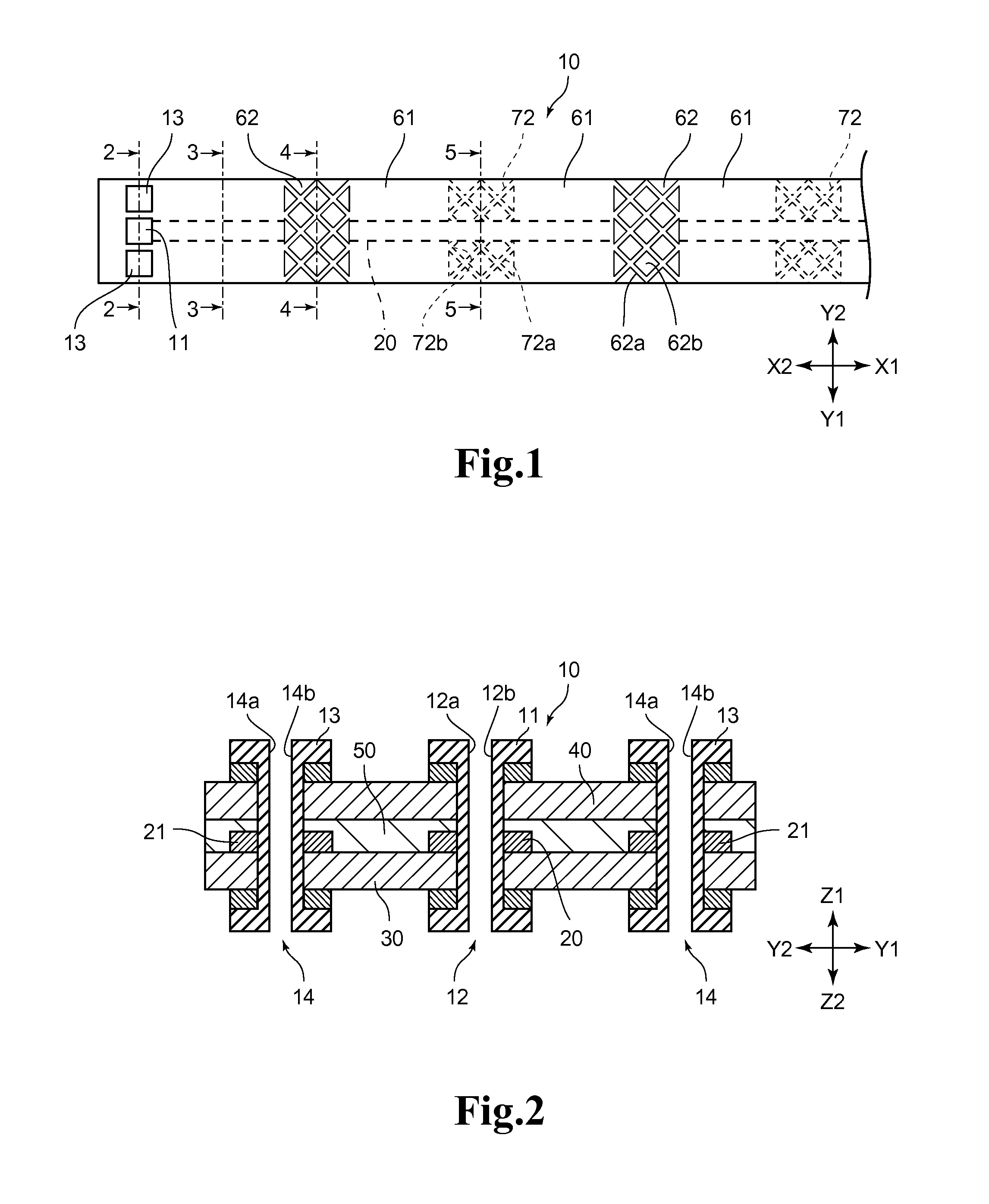
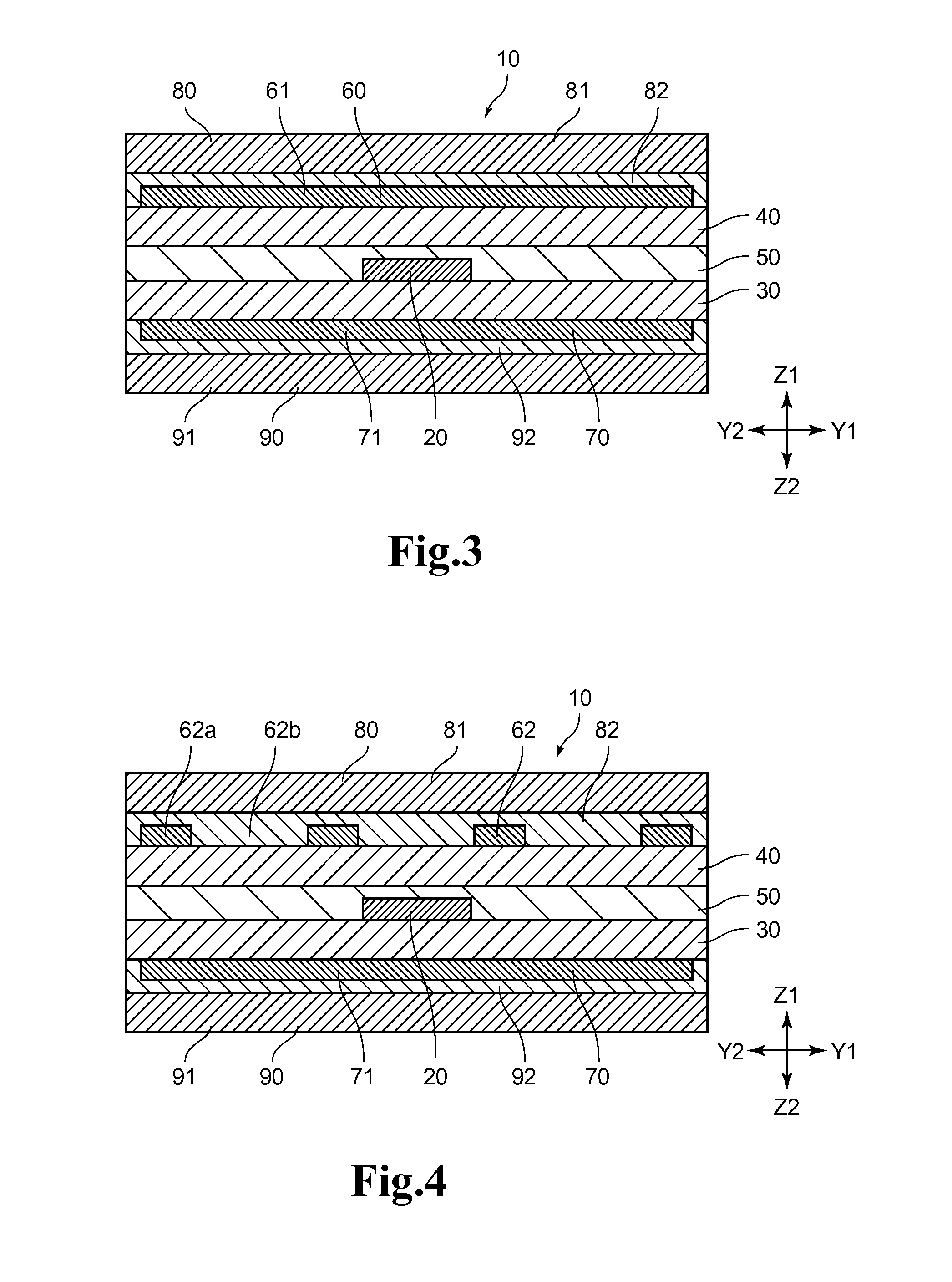
[0069]Next, the first configuration example in the arrangement of the mesh ground layers 62 and 72 in the flexible printed circuit board 10 will be described. As illustrated in FIG. 1, the mesh ground layers 62 and 72 are provided so as to exist on the front surface side and the rear surface side of the flexible printed circuit board 10 in an alternate manner. Specifically, in the vicinity of the line 4-4 in FIG. 1, the mesh ground layers 62 and 72 are arranged on the front surface side of the flexible printed circuit board 10, as illustrated in FIG. 4. Meanwhile, in the vicinity of the line 5-5 in FIG. 1, the mesh ground layers 62 and 72 are arranged on the rear surface side of the flexible printed circuit board 10, as illustrated in FIG. 5.

[0070]The arrangement as described above will be explained based on FIG. 6. FIG. 6 is a side view illustrating a shape of the flexible printed circuit board 10 after the molding. As illustrated in FIG. 6, the flexible printed circuit board 10 af...

second configuration example

[0081]Next, a second configuration example in the arrangement of the mesh ground layers 62 (mesh ground layers 72) in the flexible printed circuit board 10 will be described. FIG. 8 is a plan view illustrating the second configuration example of the flexible printed circuit board 10 before molding, which corresponds to a modified example of FIG. 1. Note that in the following explanation regarding the flexible printed circuit board 10 in the second configuration example, explanation of a part common to that of the flexible printed circuit board 10 in the first configuration example will be omitted.

[0082]As illustrated in FIG. 8, configurations of most of the parts of the flexible printed circuit board 10 in the second configuration example are common to those of the flexible printed circuit board 10 in the first configuration example as illustrated in FIG. 1. However, the arrangement of the mesh ground layers 62 (mesh ground layers 72) in the flexible printed circuit board 10 in the ...

modified example

[0131]Although one embodiment of the present invention is described as above, the present invention is not limited to this, and can be modified in various ways. This will be described hereinafter.

[0132]In the above-described embodiment, only one of the signal line 20 is illustrated. However, the number of the signal line 20 is not limited to one, and two or more of the signal lines 20 may also exist as long as they configure the strip line transmission path.

[0133]Further, in the second configuration example in the above-described embodiment, the mesh ground layers 72 are positioned at the curved portions PL2 on the inside diameter side of the pivot part of the external device such as the joint or the like of the arms of the robot or the like. Specifically, it is configured such that the mesh ground layers 62 positioned at the curved portions PL2 on the outside diameter side of the pivot part do not exist. However, it is also possible to adopt a configuration in which the mesh ground...


PUM

PropertyMeasurementUnit
Flexibilityaaaaaaaaaa

Abstract

A flexible printed circuit board having at least a set of strip line transmission path by being provided with a signal line, and a pair of ground layers and, includes a pleated part PL having a plurality of curved portions which are curved so as to be opened or closed, in which in the ground layers, mesh ground layers in which conductive portions are provided in a mesh shape, and solid ground layers in which the conductive portions are provided in a planar state, are provided, in which the mesh ground layers are arranged on an outer peripheral side of the curved portions PL2, and the solid ground layers are arranged on an inner peripheral side of the curved portions.

Description

CROSS REFERENCE TO RELATED APPLICATIONS[0001]This application is a continuation in part application under 35 U.S.C. §120 of PCT / JP2014 / 082978, filed Dec. 12, 2014 which is incorporated herein reference and which claimed priority to Japanese Application No. 2014-123753, filed Jun. 16, 2014. The present application likewise claims priority under 35 U.S.C. §119 to Japanese Application No. 2014-123753, filed Jun. 16, 2014, the entire content of which is also incorporated herein by reference.TECHNICAL FIELD[0002]The present invention relates to a flexible printed circuit board and a manufacturing method of a flexible printed circuit board.BACKGROUND ART[0003]In recent years, development in robots is remarkable such that robots performing a variety of motions are appearing. Further, a wearable electronic device capable of being attached to a human body or clothing is also being developed and put to practical use in various devices. Although, in these robots and wearable electronic devices...

Claims


Application Information

Patent Timeline
IPC IPC(8): H01P11/00H01P3/08H05K1/02H05K1/11H05K3/00H05K3/42
CPCH01P3/003H01P11/003H05K3/42H05K1/115H05K3/0061H05K1/028H05K1/0227H05K2201/093H01P3/085H05K1/0225H05K2201/0129H05K2201/09681
Inventor MATSUDA, FUMIHIKO
Owner NIPPON MEKTRON LTD
Why Eureka
Try Eureka