Light emitting device
a technology light source, which is applied in the direction of electroluminescent light source, thermoelectric device, electric lighting source, etc., can solve the problem of not being able to suppress the reflection of external light in the region of light emitting device, and achieve the effect of suppressing the reflection of external ligh
- Summary
- Abstract
- Description
- Claims
- Application Information
AI Technical Summary
Benefits of technology
Problems solved by technology
Method used
Image
Examples
embodiment
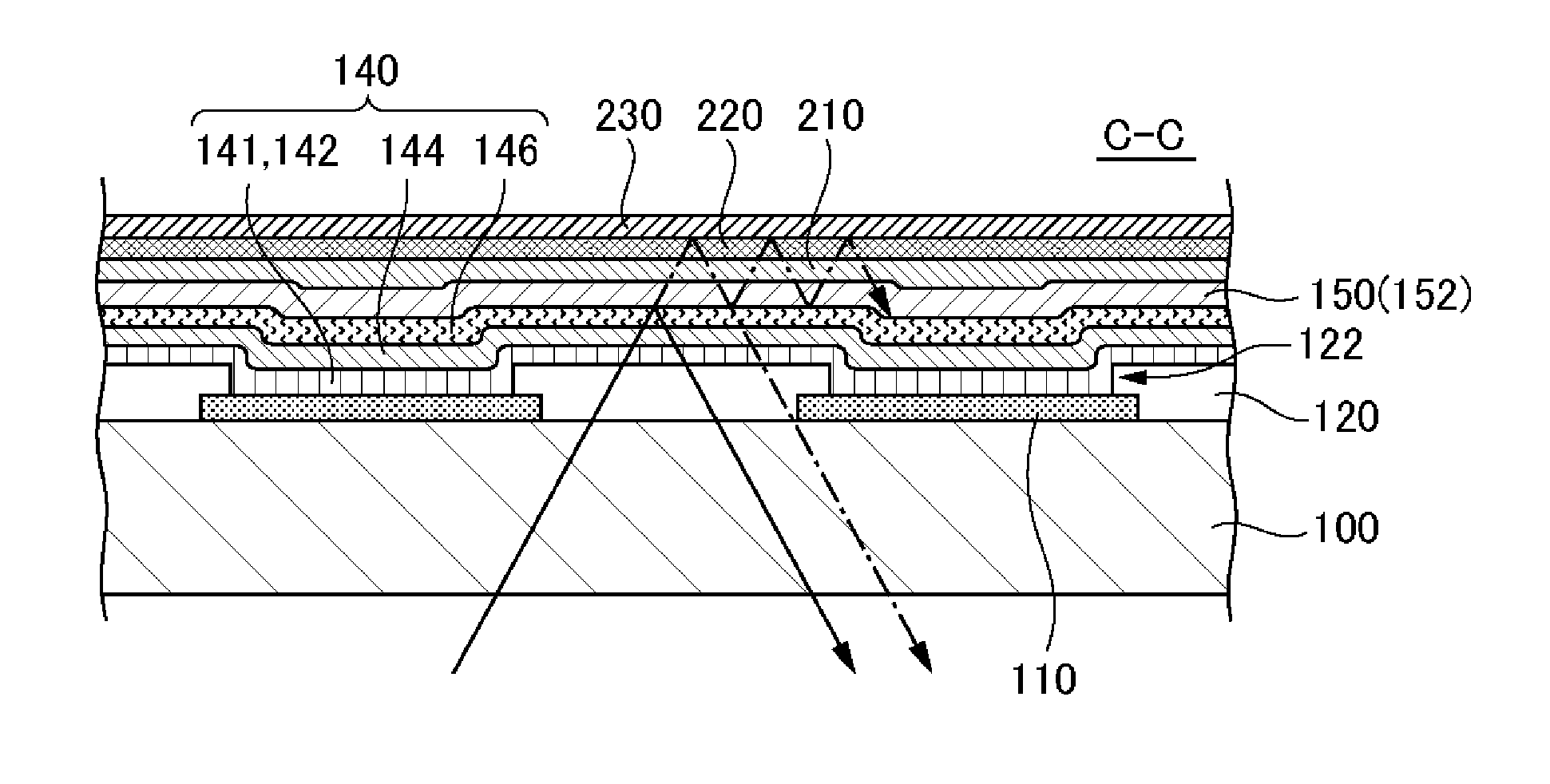
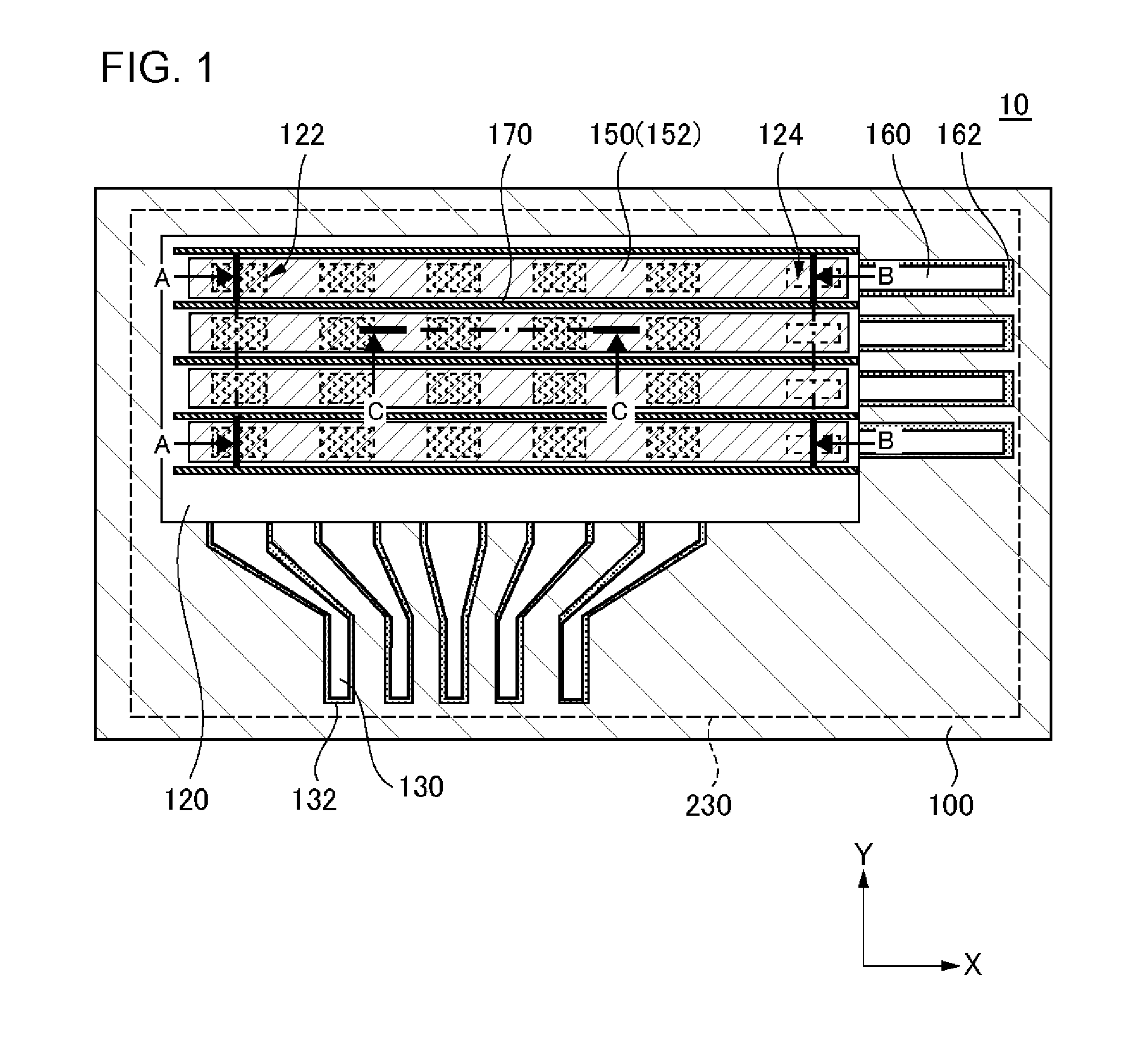
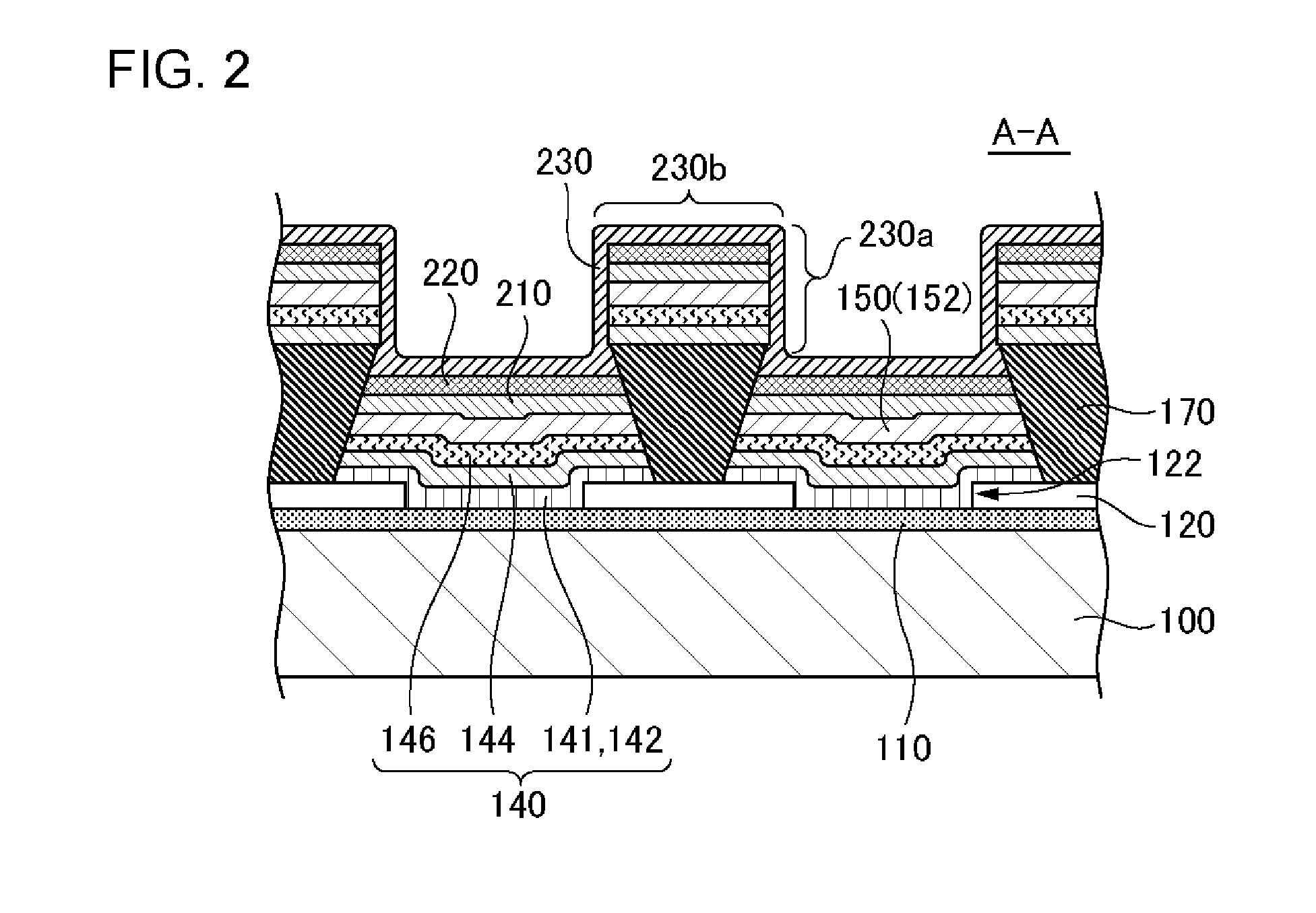
[0022]FIG. 1 is a plan view illustrating a configuration of a light emitting device 10 according to an embodiment. FIG. 2 is a cross-sectional view taken along line A-A of FIG. 1, FIG. 3 is a cross-sectional view taken along line C-C of FIG. 1, and FIG. 4 is a cross-sectional view taken along line B-B of FIG. 1.
[0023]The light emitting device 10 is, for example, a display or an illumination device. When the light emitting device 10 is an illumination device, the light emitting device 10 may be a device that realizes color rendering properties by including a first electrode 110, an organic layer 140, and a second electrode 150. The light emitting device 10 as an illumination device may be configured such that the first electrode 110, the organic layer 140, and the second electrode 150 are formed to be flush with each other without forming a partition wall 170 as a structure described later. Meanwhile, in the following description, a case where the light emitting device 10 is a displa...
example 1
[0067]FIG. 6 is a plan view illustrating a configuration of the light emitting device 10 according to Example 1. FIG. 7 is a cross-sectional view taken along line A-A of FIG. 6, and FIG. 8 is a cross-sectional view taken along line C-C of FIG. 6. The light emitting device 10 according to the present example has the same configuration as that of the light emitting device 10 according to the embodiment, except for the following points.
[0068]First, the insulating layer 120 is provided only below the partition wall 170, and covers the upper surface of the first electrode 110, but does not cover the lateral side. That is, the lateral side of the first electrode 110 is exposed. For this reason, there is a non-formation region of the insulating film layer 120 in which the insulating layer 120 is not provided between two first electrodes 110 adjacent to each other. That is, the non-light-emitting portion 104 between the two first electrodes 110 adjacent to each other and between the insulat...
example 2
[0074]FIGS. 9 and 10 are cross-sectional views illustrating a configuration of a light emitting device 10 according to Example 2. FIG. 9 corresponds to FIG. 2 of the embodiment, and FIG. 10 corresponds to FIG. 3 of the embodiment. The light emitting device 10 according to Example 2 has the same configuration as that of the light emitting device 10 according to the embodiment or Example 1, except that the light-transmitting film 210 is not included therein.
[0075]In the present example, the laminated structure of the second electrode 150 and the reflective film 220 is formed not only in the light-emitting portion 102, but also in the non-light-emitting portion 104. Therefore, it is possible to suppress the reflection of external light in each of the light-emitting portion 102 and the non-light-emitting portion 104.
PUM
 Abstract
Description
Claims
Application Information


