
Display device including organic layer including pigment or dye and method of manufacturing thereof

a technology of display device and organic layer, which is applied in the direction of organic semiconductor device, solid-state device, instrument, etc., can solve the problems of reducing light utilization efficiency, difficulty in realizing full black tone, and reducing contrast thereof, so as to prevent external light reflection, improve color purity, and reduce light utilization efficiency

Active Publication Date: 2019-12-17
SAMSUNG DISPLAY CO LTD
View PDF12 Cites 0 Cited by
  • Summary
  • Abstract
  • Description
  • Claims
  • Application Information

AI Technical Summary

Benefits of technology

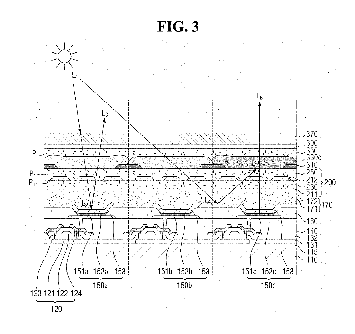
This patent relates to a display device that can improve color purity, suppress the reflection of external light, and maximize the efficiency of light emitted from a light-emitting element to improve luminance and reduce power consumption. The technical effects of this invention include the use of a polarizing element and a phase delay element on a light-emitting layer to prevent reflection, and the optimization of the display device's configuration to improve light utilization efficiency. The patent also describes a method for manufacturing the display device, which follows the same technical principles.

Problems solved by technology

Therefore, when the organic light-emitting display device is used in a bright place, it may be difficult to realize a full black tone due to the reflection of external light, and the contrast thereof may be lowered.
However, when the polarizing element is disposed on the light-emitting layer, there is a limitation in that at least 50% of the light emitted from the light-emitting layer is absorbed by the polarizing element, and thus light utilization efficiency is lowered.

Method used


Image

  • Display device including organic layer including pigment or dye and method of manufacturing thereof
  • Display device including organic layer including pigment or dye and method of manufacturing thereof
  • Display device including organic layer including pigment or dye and method of manufacturing thereof

Examples


Embodiment Construction

[0037]Features of the invention and methods of accomplishing the same may be understood more readily by reference to the following detailed description of preferred embodiments and the accompanying drawings. The invention may, however, be embodied in many different forms and should not be construed as being limited to the embodiments set forth herein. Rather, these embodiments are provided so that this disclosure will be thorough and complete and will fully convey the concept of the invention to those skilled in the art, and the invention will only be defined by the appended claims.

[0038]It will be understood that when an element or layer is referred to as being “on,”“connected to” or “coupled to” another element or layer, the element or layer can be directly on, connected or coupled to another element or layer or intervening elements or layers. In contrast, when an element is referred to as being “directly on,”“directly connected to” or “directly coupled to” another element or laye...


PUM


Abstract

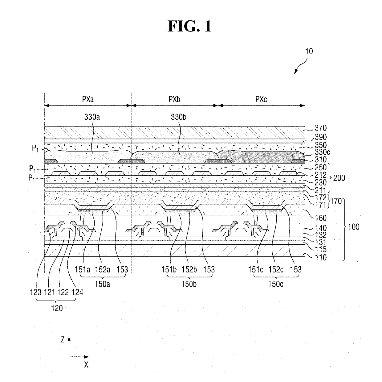
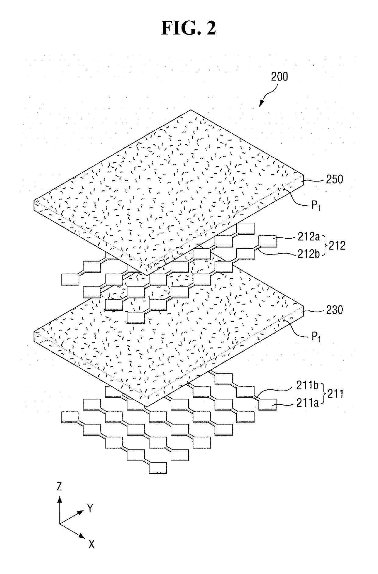
A display device, in which a first pixel and a second pixel are defined, includes: a display panel including a base substrate and a light-emitting element disposed on the base substrate; a color filter layer disposed over the display panel and including a first color filter disposed in the first pixel and a second color filter disposed in the second pixel; and a first organic layer disposed over the display panel, and including a pigment or a dye. The first pixel displays a first color, and the second pixel displays a second color different from the first color. The organic layer is integrally formed over the first pixel and the second pixel.

Description

[0001]This application claims priority to Korean Patent Application No. 10-2017-0002876, filed on Jan. 9, 2017, and all the benefits accruing therefrom under 35 U.S.C. § 119, the content of which in its entirety is herein incorporated by reference.BACKGROUND1. Field[0002]Embodiments of the invention relate to a display device and a method of manufacturing the display device.2. Description of the Related Art[0003]A self-emission type display device, such as an organic light-emitting display device, may include an organic light-emitting element. The organic light-emitting element may include two electrodes facing each other and an organic light-emitting layer interposed therebetween. Electrons and holes provided from the two electrodes are recombined in the organic light-emitting layer to generate excitons, and the generated excitons are shifted from an excited state to a ground state, to emit light.[0004]Since the organic light-emitting display device may not use an additional light ...

Claims


Application Information

Patent Timeline
Patent Type & Authority Patents(United States)
IPC IPC(8): H01L27/32H01L51/00G06F3/041G06F3/044H01L35/24H01L29/08H01L51/56H01L51/52H10N10/856
CPCH01L27/322H01L51/56H01L51/5284G06F3/0412H01L51/5253H01L51/5246G06F2203/04111H01L2227/323H01L2251/5369G06F3/044H01L27/3211G06F2203/04103H01L27/323H01L27/3244G06F3/0446G06F3/0445H10K59/35H10K59/38H10K59/40H10K59/12H10K2102/331H10K59/873H10K59/8792H10K2102/361H10K50/844H10K50/865H10K50/8426H10K71/00H10K59/1201
Inventor KIM, SU JEONGLEE, YUI KUHUH, CHUL
Owner SAMSUNG DISPLAY CO LTD
Learn More