Integrated bio-chip and method of fabricating the integrated bio-chip

a biochip and integrated technology, applied in the field of integrated biochips, can solve the problems of large detection apparatuses, complex, and high cost of current detection apparatuses, and achieve the effects of detection results, and improving the accuracy of detection

Inactive Publication Date: 2010-08-12
SAMSUNG ELECTRONICS CO LTD
View PDF13 Cites 67 Cited by
  • Summary
  • Abstract
  • Description
  • Claims
  • Application Information

AI Technical Summary

Benefits of technology

[0047]In one embodiment, the forming of the cover glass may further include an anti-excitation light reflection layer that prevents the excitation light from being reflected on an outer surface of the cover glass.

Problems solved by technology

The fluorescence obtained by irradiating the predetermined excitation light onto the fluorescent material tagged on the bio-materials is much weaker than the excitation light used for irradiation of the fluorescent material, and thus may obscure fluorescence detection.
In addition, current detection apparatuses use a scanner-type photodetector that is large, complex, and expensive, and thus, a compact bio-chip and a detection apparatus having the same would be an improvement.

Method used


Image

  • Integrated bio-chip and method of fabricating the integrated bio-chip
  • Integrated bio-chip and method of fabricating the integrated bio-chip
  • Integrated bio-chip and method of fabricating the integrated bio-chip

Examples


Embodiment Construction

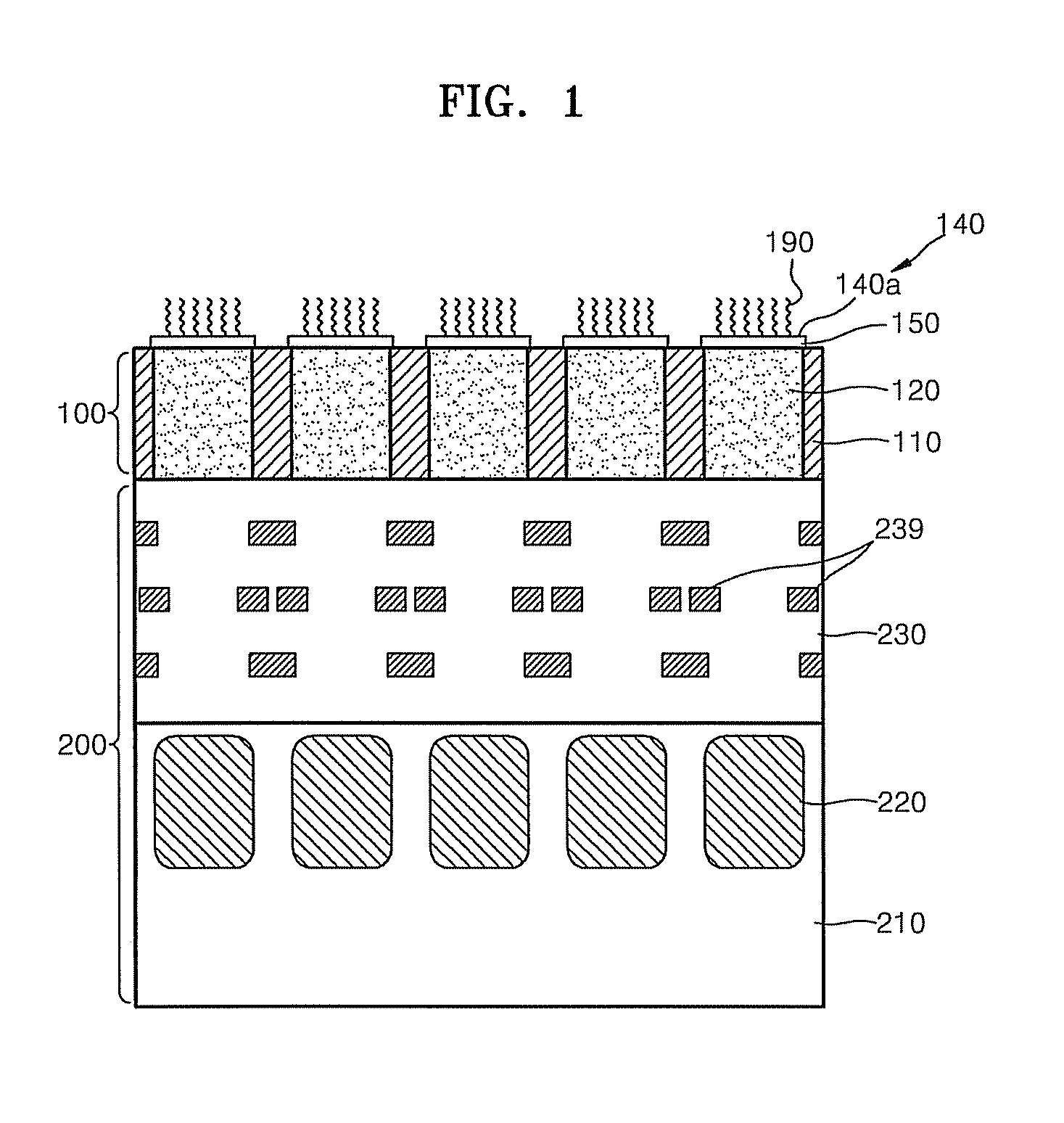
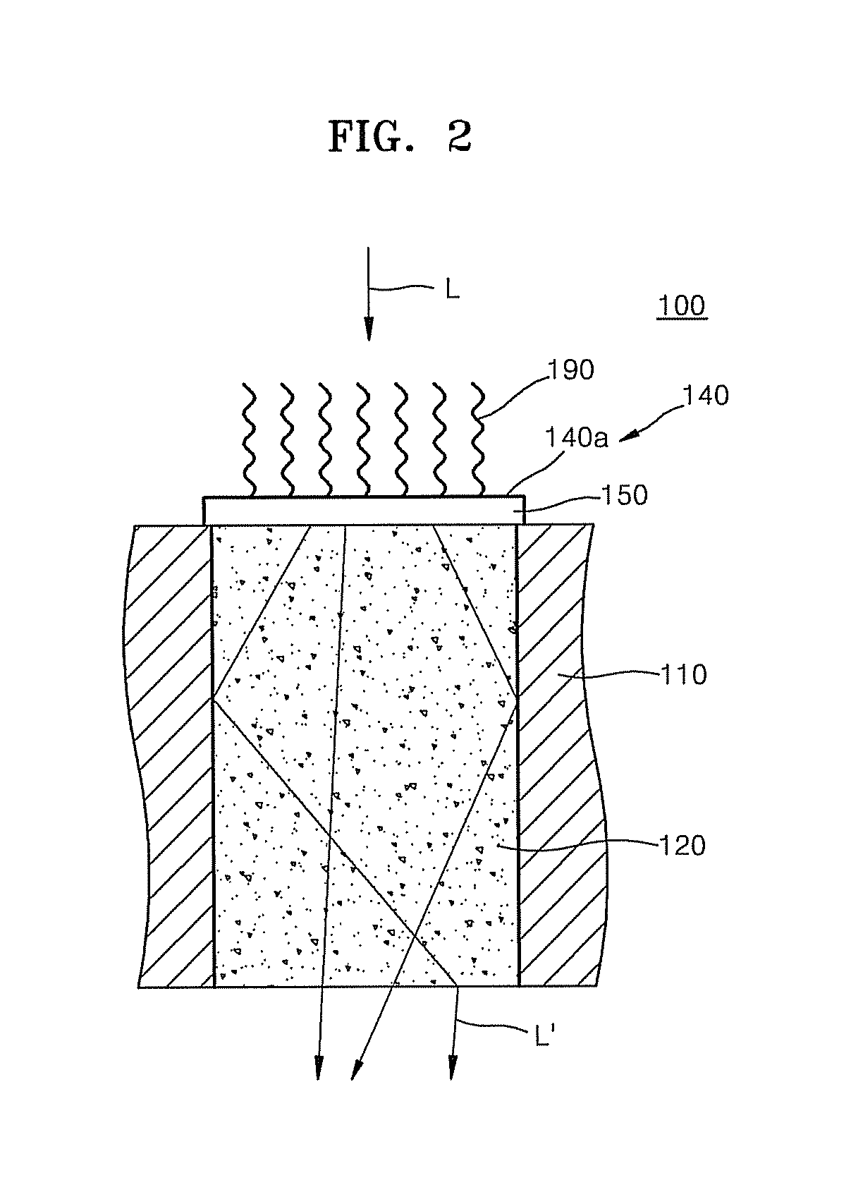
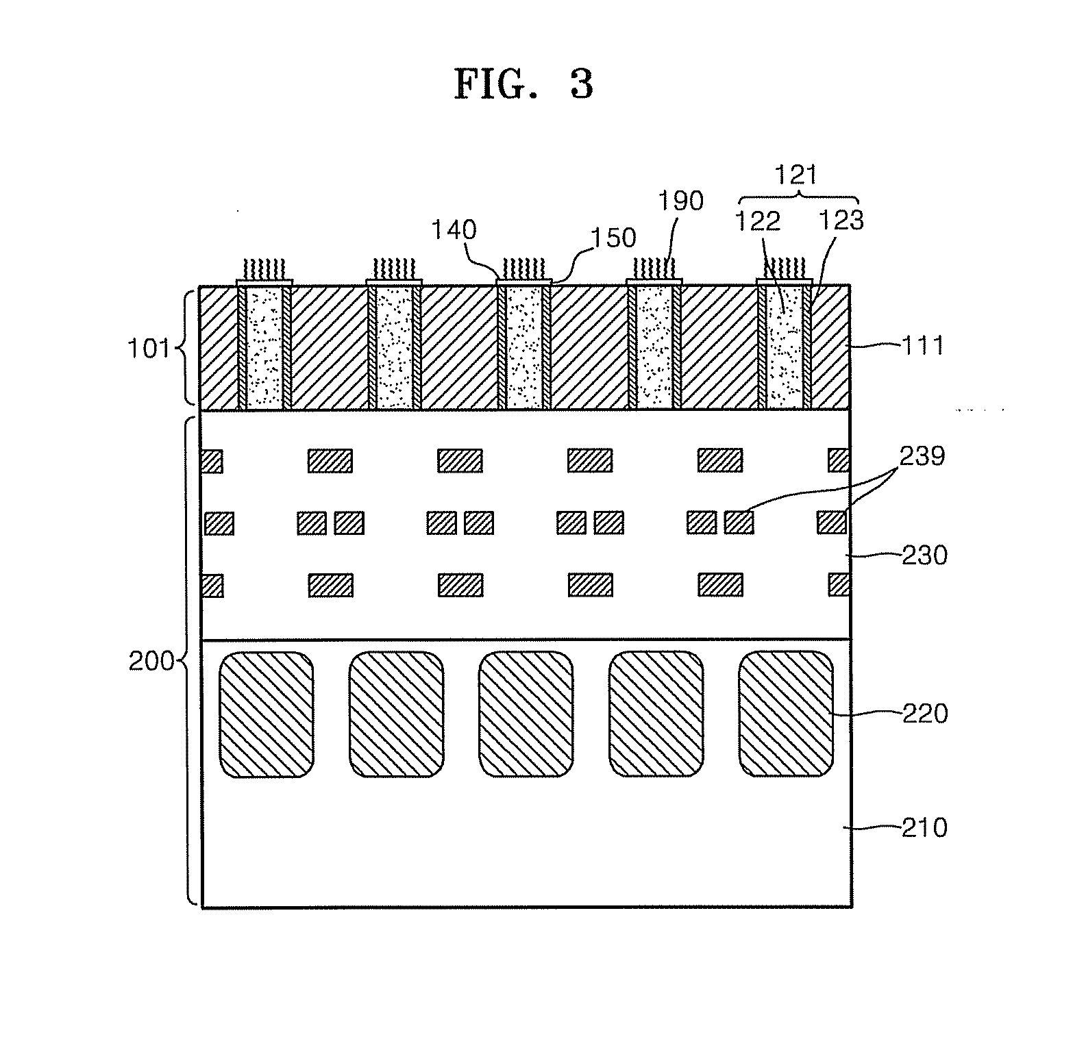
[0070]Embodiments now will be described more fully hereinafter with reference to the accompanying drawings, in which embodiments are shown. These embodiments may, however, be embodied in many different forms and should not be construed as limited to the embodiments set forth herein. Rather, these embodiments are provided so that this disclosure will be thorough and complete, and will fully convey the scope of the disclosure to those skilled in the art. Like reference numerals refer to like elements throughout.

[0071]It will be understood that when an element is referred to as being “on” another element, it can be directly on the other element or intervening elements may be present therebetween. In contrast, when an element is referred to as being “directly on” another element, there are no intervening elements present. As used herein, the term “and / or” includes any and all combinations of one or more of the associated listed items.

[0072]It will be understood that, although the terms ...


PUM

PropertyMeasurementUnit
wavelengthaaaaaaaaaa
fluorescentaaaaaaaaaa
refractive indexaaaaaaaaaa

Abstract

An integrated bio-chip includes; a sample detection portion including at least one light receiving device which detects fluorescent light emitted from at least one sample, a light transfer portion disposed on a light incident surface of the sample detection portion, and which includes at least one excitation light absorbing waveguide which absorbs an excitation light and transmits the fluorescent light emitted from the at least one sample, and a sample reaction portion disposed adjacent to an incident end of the at least one excitation light absorbing waveguide, and including at least one reaction region on which the at least one sample is attached, wherein the sample detection portion, the light transfer portion, and the sample reaction portion are integrally coupled to each other as a single component.

Description

CROSS-REFERENCE TO RELATED APPLICATIONS[0001]This application claims priority to Korean Patent Application No. 10-2009-0011211, filed on Feb. 11, 2009, Korean Patent Application No. 10-2009-0011212, filed on Feb. 11, 2009, Korean Patent Application No. 10-2009-0011213, filed on Feb. 11, 2009 and Korean Patent Application No. 10-2009-0011216, filed on Feb. 11, 2009, and all the benefits accruing therefrom under 35 U.S.C. §119, the contents of which in their entirety are herein incorporated by reference.BACKGROUND[0002]1. Field[0003]The present disclosure relates to integrated bio-chips and methods of fabricating the same, and more particularly, to integrated bio-chips used for spectroscopically detecting a sample and methods of fabricating the integrated bio-chips.[0004]2. Description of the Related Art[0005]Bio-chips typically have a structure in which very tiny, e.g., microscopic, cells are arranged on a substrate in micro-units in a matrix shape, wherein each of the cells includes...

Claims


Application Information

Patent Timeline
Patent Type & Authority Applications(United States)
IPC IPC(8): C40B40/08C40B50/14
CPCG01N21/6454
Inventor CHO, SEONG-HO
Owner SAMSUNG ELECTRONICS CO LTD
Why Eureka
Try Eureka