Display Panel, Input/output Device, and Data Processor

a technology for display panels and input/output devices, applied in the direction of static indicating devices, electric apparatus casings/cabinets/drawers, instruments, etc., to achieve the effect of high convenient or reliable, and high convenient or reliabl

Active Publication Date: 2016-03-10
SEMICON ENERGY LAB CO LTD
View PDF15 Cites 19 Cited by
  • Summary
  • Abstract
  • Description
  • Claims
  • Application Information

AI Technical Summary

Benefits of technology

[0009]An object of one embodiment of the present invention is to provide a novel display panel that is highly convenient or reliable. Another object is to provide a novel input / output device that is highly convenient or reliable. Another object is to provide a novel data processor that is highly convenient or reliable. Another object is to provide a novel display panel, a novel input / output device, a novel data processor, or a novel semiconductor device.

Problems solved by technology

For example, portable data processors are often used while being carried around by a user, and force might be accidentally applied, by dropping, to the data processors and display devices included in them.

Method used


Image

  • Display Panel, Input/output Device, and Data Processor
  • Display Panel, Input/output Device, and Data Processor
  • Display Panel, Input/output Device, and Data Processor

Examples


embodiment 1

[0049]In this embodiment, a structure of a display panel of one embodiment of the present invention will be described with reference to FIGS. 1A to 1C, FIGS. 2A to 2C, FIGS. 12A and 12B, FIGS. 13A and 13B, FIGS. 14A to 14D, FIGS. 15A and 15B and FIGS. 16A and 16B.

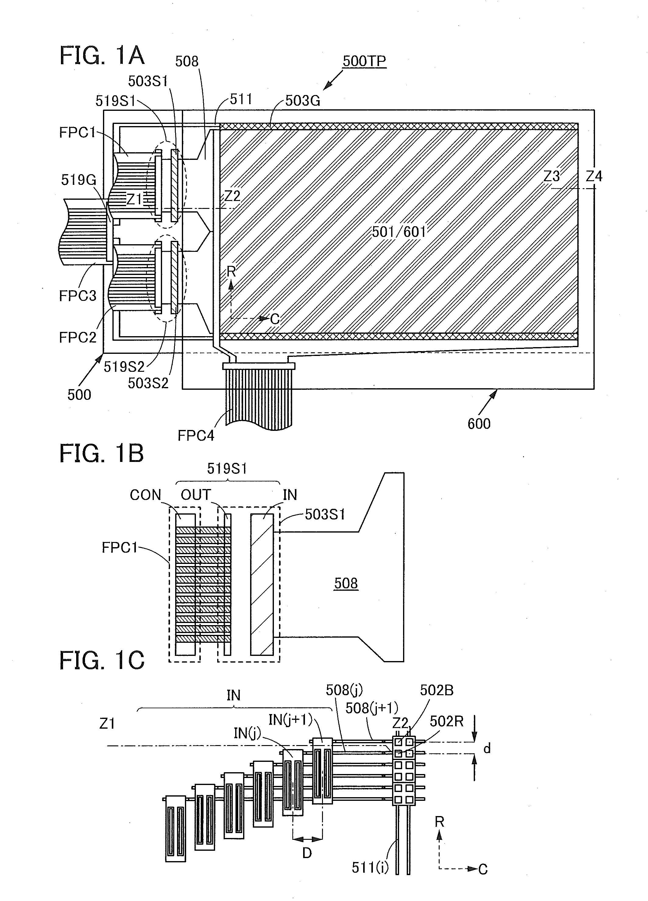
[0050]FIGS. 1A to 1C illustrate a structure of an input / output device 5001P that includes a display panel 500 of one embodiment of the present invention.

[0051]FIG. 1A is a top view illustrating the structure of the input / output device 500TP, FIG. 1B is a top view illustrating a structure of a terminal portion 519S1 included in the display panel 500, and FIG. 1C is a top view illustrating pixels, wirings, and terminals included in the display panel 500.

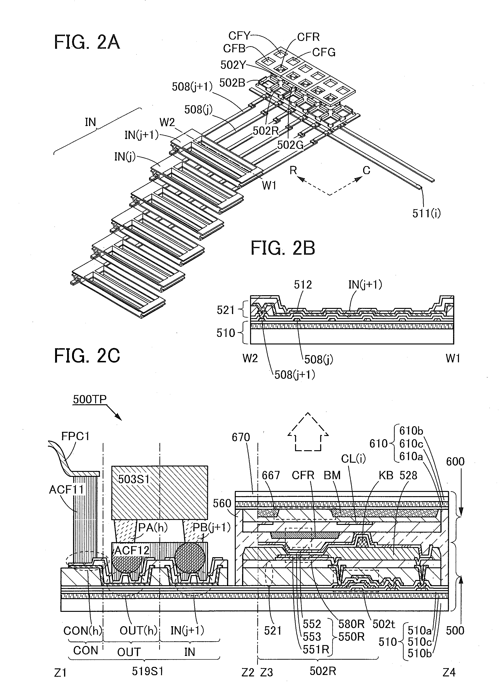
[0052]FIG. 2A is a projection view illustrating the pixels, wirings, and terminals included in the display panel 500, FIG. 2B is a cross-sectional view of a second terminal IN(j+1) taken along the line W1-W2 in FIG. 2A, and FIG. 2C is a cross-sectional view of the input / output...

embodiment 2

[0186]In this embodiment, a structure of the input / output device 500TP of one embodiment of the present invention will be described with reference to FIG. 4.

[0187]FIG. 4 is a projection view illustrating the structure of the input / output device 500TP.

[0188]The input / output device 500TP described in this embodiment includes the display panel 500 and the sensor panel 600 having a region that overlaps with the first pixel 502R and the second pixel 502B of the display panel 500.

[0189]The input / output device 500TP described in this embodiment includes the display panel 500 including the selection signal line 511(i), the first signal line 508(j) and the second signal line 508(j+1) that cross the selection signal line 511(i), the first pixel 502R that is electrically connected to the selection signal line 511(i) and the first signal line 508(j), the second pixel 502B that is electrically connected to the selection signal line 511(i) and the second signal line 508(j+1), the first terminal I...

embodiment 3

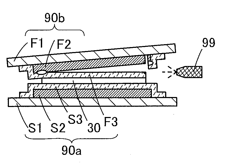
[0217]In this embodiment, a method of manufacturing a stack that can be used in the manufacture of the sensor device, input device, or input / output device of one embodiment of the present invention will be described with reference to FIGS. 5A-1 and 5A-2, FIGS. 5B-1 and 5B-2, FIG. 5C, FIGS. 5D-1 and 5D-2, and FIGS. 5E-1 and 5E-2.

[0218]FIGS. 5A-1 to 5E-2 are schematic views illustrating a process of manufacturing the stack. Cross-sectional views illustrating structures of a processed member and the stack are shown on the left side of FIGS. 5A-1 to 5E-2, and top views corresponding to the cross-sectional views except FIG. 5C are shown on the right side.

[0219]A method of manufacturing a stack 81 from a processed member 80 will be described with reference to FIGS. 5A-1 to 5E-2.

[0220]The processed member 80 includes a first substrate F1, a first separation layer F2 on the first substrate F1, a first layer F3 to be separated whose one surface is in contact with the first separation layer F...


PUM


Abstract

A novel display panel that is highly convenient or reliable, a novel input / output device that is highly convenient or reliable, or a novel data processor that is highly convenient or reliable is provided. The display panel includes a selection signal line, a first signal line and a second signal line that cross the selection signal line, a first pixel electrically connected to the selection signal line and the first signal line, a second pixel electrically connected to the selection signal line and the second signal line, a first terminal electrically connected to the first signal line, and a second terminal electrically connected to the second signal line.

Description

BACKGROUND OF THE INVENTION[0001]1. Field of the Invention[0002]One embodiment of the present invention relates to a display panel, an input / output device, or a data processor.[0003]Note that one embodiment of the present invention is not limited to the above technical field. The technical field of one embodiment of the invention disclosed in this specification and the like relates to an object, a method, or a manufacturing method. In addition, one embodiment of the present invention relates to a process, a machine, manufacture, or a composition of matter. Specific examples of the technical field of one embodiment of the present invention disclosed in this specification include a semiconductor device, a display device, a light-emitting device, a power storage device, an imaging device, a memory device, a method for driving any of them, and a method for manufacturing any of them.[0004]2. Description of the Related Art[0005]The social infrastructures relating to means for transmitting...

Claims


Application Information

Patent Timeline
Patent Type & Authority Applications(United States)
IPC IPC(8): G06F1/18G06F1/16G09G5/00
CPCG06F1/182G09G2300/0426G06F1/1601G09G5/003G06F1/1643G06F1/1652G02F1/133308G02F1/1345G02F1/13452G09G3/2096G02F1/133325G09G3/20
Inventor TAKAHASHI, KEISHISHIDO, HIDEAKIMARUYAMA, JUNYA
Owner SEMICON ENERGY LAB CO LTD
Why Eureka
Try Eureka