Display device, electronic device, and method for manufacturing display device and electronic device

a display device and electronic device technology, applied in semiconductor devices, diodes, instruments, etc., can solve the problems of device including a reflective liquid crystal display element having problems of dark display, consuming more power, and reducing visibility, so as to achieve high luminance, reduce visibility, and high visibility

Inactive Publication Date: 2017-05-04
SEMICON ENERGY LAB CO LTD
View PDF2 Cites 15 Cited by
  • Summary
  • Abstract
  • Description
  • Claims
  • Application Information

AI Technical Summary

Benefits of technology

[0006]A display device including a light-emitting element or a transmissive liquid crystal display element has a problem that the visibility is reduced when displaying images in a bright environment, such as under strong external light. In addition, when the display device outputs high luminance for high visibility in the bright environment, it consumes more power. In contrast, a display device including a reflective liquid crystal display element has problems of dark display, low color reproducibility, and low visibility when displaying images in a dark environment. Accordingly, a convenient display device with high visibility and low power consumption both in bright and dark environments is required.
[0007]In view of the above, an object of one embodiment of the present invention is to provide a display device with high visibility that is highly convenient. Another object of one embodiment of the present invention is to provide a display device with low power consumption. Another object of one embodiment of the present invention is to provide a display device with high color reproducibility. Another object of one embodiment of the present invention is to provide a highly reliable display device. Another object of one embodiment of the present invention is to provide a novel display device. Another object of one embodiment of the present invention is to provide a method for manufacturing a novel display device.
[0020]One embodiment of the present invention provides a display device with high visibility that is highly convenient, a display device with low power consumption, a display device with high color reproducibility, a highly reliable display device, a novel display device, or a method for manufacturing a novel display device.

Problems solved by technology

A display device including a light-emitting element or a transmissive liquid crystal display element has a problem that the visibility is reduced when displaying images in a bright environment, such as under strong external light.
In addition, when the display device outputs high luminance for high visibility in the bright environment, it consumes more power.
In contrast, a display device including a reflective liquid crystal display element has problems of dark display, low color reproducibility, and low visibility when displaying images in a dark environment.

Method used


Image

  • Display device, electronic device, and method for manufacturing display device and electronic device
  • Display device, electronic device, and method for manufacturing display device and electronic device
  • Display device, electronic device, and method for manufacturing display device and electronic device

Examples


embodiment 1

[0105]In this embodiment, display devices of embodiments of the present invention will be described below with reference to FIGS. 1A, 1B-1, and 1B-2, FIGS. 2A to 2C, FIG. 3, FIGS. 4A, 4B-1, and 4B-2, FIGS. 5A and 5B, FIGS. 6A and 6B, FIGS. 7A and 7B, FIGS. 8A and 8B, FIGS. 9A and 9B, FIGS. 10A and 10B, FIG. 11, FIG. 12, FIG. 13, FIG. 14, FIG. 15, FIGS. 16A and 16B, FIGS. 17A and 17B, FIGS. 18A and 18B, FIGS. 19A and 19B, FIG. 20, FIG. 21, FIGS. 22A and 22B, FIG. 23, FIGS. 24A and 24B, and FIGS. 25A and 25B.

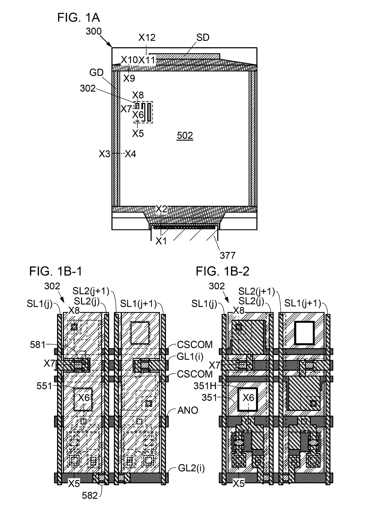
[0106]FIG. 1A is a bottom view illustrating the structure of a display device 300 of one embodiment of the present invention. FIG. 1B-1 is a bottom view illustrating part of FIG. 1A. FIG. 1B-2 is a bottom view omitting some components illustrated in FIG. 1B-1.

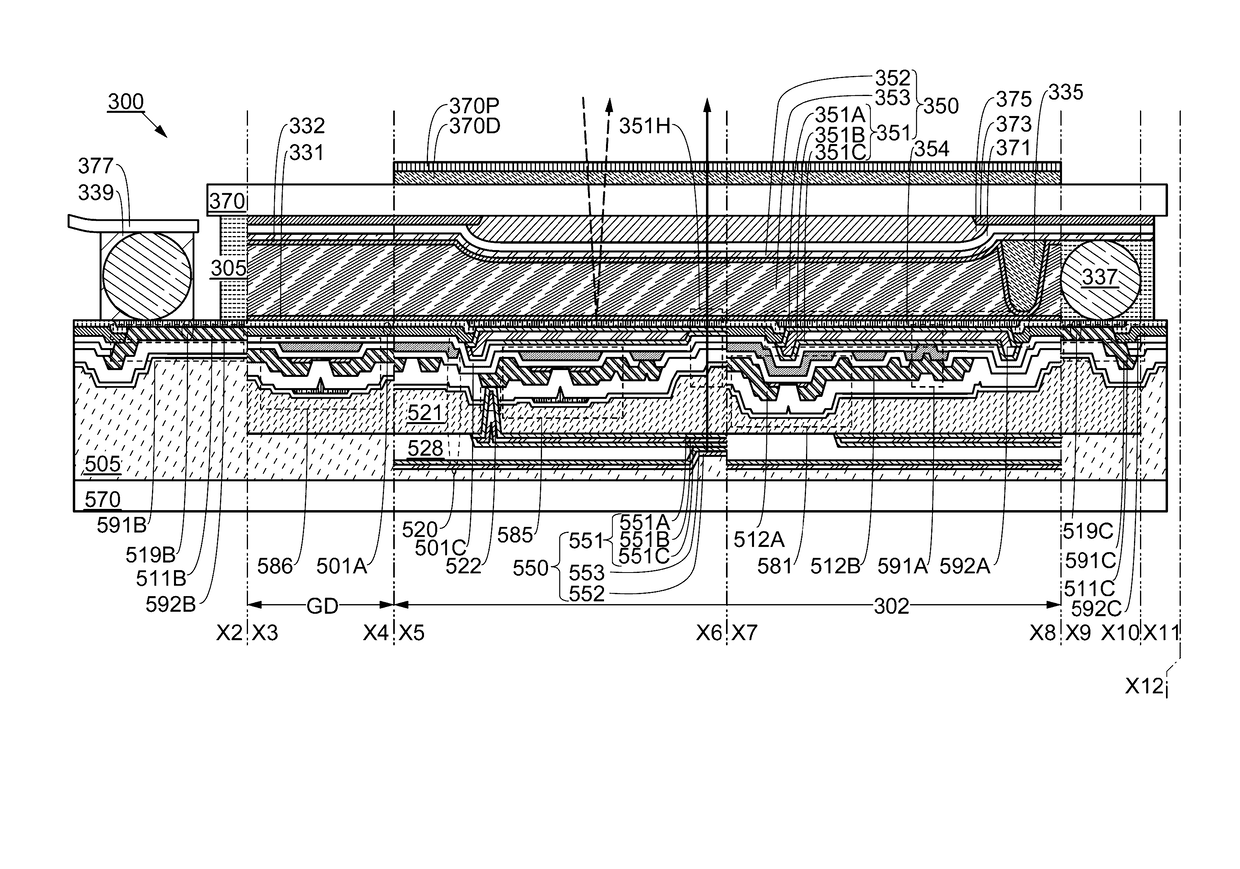
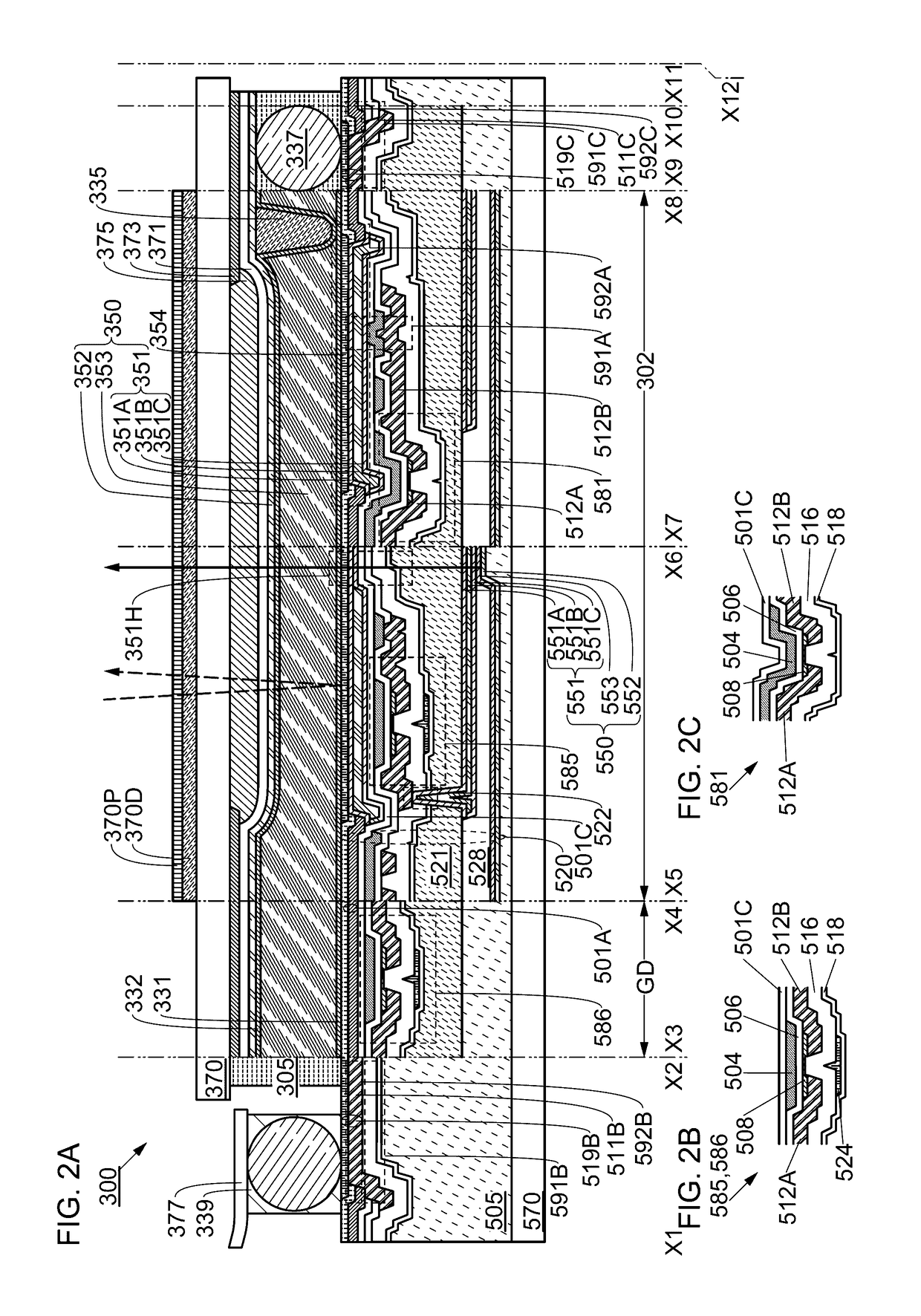
[0107]FIGS. 2A to 2C are cross-sectional views illustrating the structure of the display device 300 of one embodiment of the present invention. FIG. 2A is a cross-sectional view taken along dashed-dotted lines X1-X2, X3-X4, X...

structure example 1

[0136]FIG. 24A is a cross-sectional view of a light-emitting element of the display device 300 of one embodiment of the present invention. A light-emitting element 550A that can be used as the second display element 550 includes a pair of electrodes (the electrodes 551 and 552) and the light-emitting layer 553 provided between the pair of electrodes. The light-emitting element 550A preferably includes a hole-injection layer 561, a hole-transport layer 562, an electron-transport layer 568, and an electron-injection layer 569 in addition to the light-emitting layer 553.

[0137]The structure of the light-emitting element 550A is not limited thereto, and a structure including at least one layer selected from the hole-injection layer 561, the hole-transport layer 562, the electron-transport layer 568, and the electron-injection layer 569 may be employed. Alternatively, the light-emitting element used as the second display element 550 may include a layer which is capable of lowering a hole-...

structure example 2

[0176]The light-emitting element used as the second display element 550 may be formed by a color filter method. A light-emitting element 550C and a light-emitting element 550D illustrated in FIGS. 25A and 25B as examples are each a light-emitting element in which light-emitting layers having a function of emitting light of different colors are formed in common in the regions 571R, 571G, and 571B.

[0177]It is not necessary to use a shadow mask in steps of forming the light-emitting elements 550C and 550D; therefore, the light-emitting elements can be fabricated with high productivity.

[0178]In each of the light-emitting elements 550C and 550D, the optical length between the electrodes 551 and 552 is adjusted with the microcavity structure, resulting in high light extraction efficiency.

[0179]Note that in each of the light-emitting elements 550C and 550D, by adjusting the thicknesses of the conductive film 551C in each region (the region 571R, 571G, or 571B), light emitted from the light...


PUM

PropertyMeasurementUnit
conductiveaaaaaaaaaa
semiconductoraaaaaaaaaa
power consumptionaaaaaaaaaa

Abstract

A novel display device that is highly convenient with low power consumption is provided. The display device includes a display element including a liquid crystal layer, a display element including a light-emitting layer, a first transistor, and a second transistor. The first transistor is electrically connected to an electrode of the display element including the liquid crystal layer, and the second transistor is electrically connected to an electrode of the display element including the light-emitting layer. The electrode of the display element including the liquid crystal layer and the electrode of the display element including the light-emitting layer each include a reflective film and a conductive film. The reflective film of the display element including the liquid crystal layer has a region containing a metal contained in the reflective film of the display element including the light-emitting layer.

Description

TECHNICAL FIELD[0001]One embodiment of the present invention relates to a display device or an electronic device including the display device, and a manufacturing method of the display device and the electronic device.[0002]Note that one embodiment of the present invention is not limited to the above technical field. The technical field of one embodiment of the invention disclosed in this specification and the like relates to an object, a method, or a manufacturing method. In addition, one embodiment of the present invention relates to a process, a machine, manufacture, or a composition of matter. Specifically, examples of the technical field of one embodiment of the present invention disclosed in this specification include a semiconductor device, a display device, a liquid crystal display device, a light-emitting device, a lighting device, a power storage device, a memory device, a method for driving any of them, and a method for manufacturing any of them.BACKGROUND ART[0003]There ...

Claims


Application Information

Patent Timeline
Patent Type & Authority Applications(United States)
IPC IPC(8): G02F1/1335H01L27/32G02F1/1343H01L27/15
CPCG02F1/133553H01L27/15H01L27/3267H01L27/3232G02F1/134309G02F1/1336G02F2201/122H01L29/45H01L51/5218H01L51/5231H01L33/405G02F2202/16G02F2203/02H01L29/7869G02F2201/44H01L27/1225H10K59/50H10K59/128H10K50/826H10K50/818
Inventor SASAKI, TOSHIKISEO, SATOSHIOHSAWA, NOBUHARUYOKOYAMA, KOHEIJINBO, YASUHIRO
Owner SEMICON ENERGY LAB CO LTD
Why Eureka
Try Eureka