Display Module and Method for Manufacturing Display Module

a display module and display module technology, applied in the direction of sustainable manufacturing/processing, final product manufacturing, thermoelectric devices, etc., can solve the problems of impaired functions of some functional elements, and achieve the effect of high convenient or reliable display modules and highly convenient or reliable methods for manufacturing display modules

Inactive Publication Date: 2016-06-02
SEMICON ENERGY LAB CO LTD
View PDF10 Cites 16 Cited by
  • Summary
  • Abstract
  • Description
  • Claims
  • Application Information

AI Technical Summary

Benefits of technology

[0007]An object of one embodiment of the present invention is to provide a novel, highly convenient or reliable display module. Another object of one embodiment of the present invention is to provide a novel, highly convenient or

Problems solved by technology

Functions of some functional elements ar

Method used


Image

  • Display Module and Method for Manufacturing Display Module
  • Display Module and Method for Manufacturing Display Module
  • Display Module and Method for Manufacturing Display Module

Examples


embodiment 1

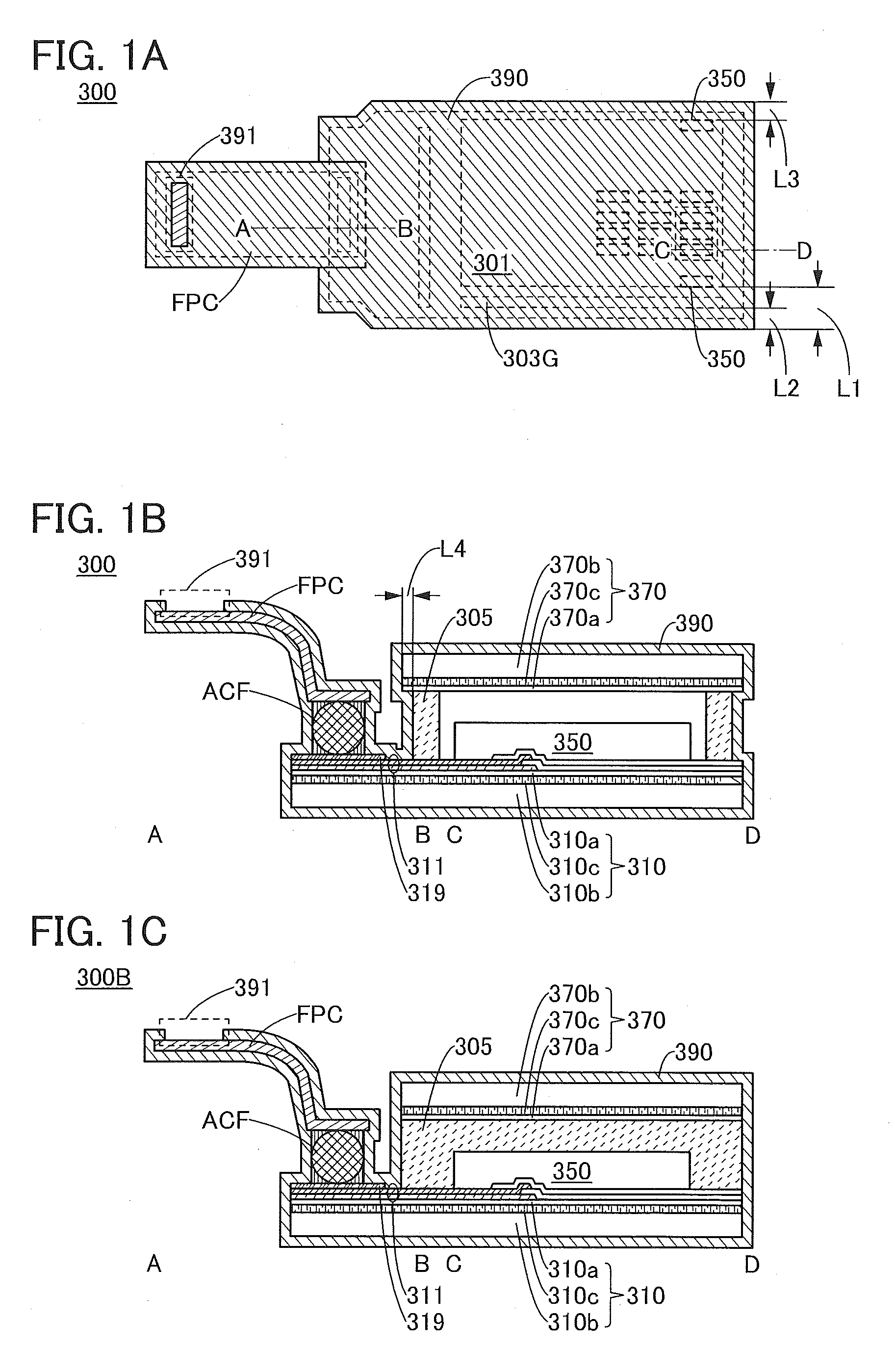
[0069]In this embodiment, a structure of a display module of one embodiment of the present invention will be described with reference to FIGS. 1A to 1C.

[0070]FIGS. 1A to 1C illustrate the structure of the display module of one embodiment of the present invention. FIG. 1A is a top view of a display module 300 of one embodiment of the present invention, and FIG. 1B is a cross-sectional view taken along the lines A-B and C-D in FIG. 1A.

[0071]FIG. 1C is a cross-sectional view illustrating a structure of a display module 300B which has a structure different from the display module 300 illustrated in FIG. 1B.

[0072]The display module 300 described in this embodiment includes a terminal 319, a first base 310 which supports the terminal 319, a second base 370 which has a region overlapping with the first base 310, a bonding layer 305 which has a function of bonding the first base 310 and the second base 370, a display element 350 which is provided between the first base 310 and the second ba...

embodiment 2

[0163]In this embodiment, a structure of a display panel of one embodiment of the present invention will be described with reference to FIGS. 3A to 3C.

[0164]FIGS. 3A to 3C illustrate the structure of the display panel of one embodiment of the present invention. FIG. 3A is a top view of a display panel 300P of one embodiment of the present invention, and FIG. 3B is a cross-sectional view taken along the lines A-B and C-D in FIG. 3A.

[0165]FIG. 3C is a cross-sectional view illustrating a structure of a display panel 300PB which has structure different from the display panel 300P illustrated in FIG. 3B.

[0166]The display panel 300P described in this embodiment includes the terminal 319, the first base 310 which is flexible and supports the terminal 319, the second base 370 which is flexible and has a region overlapping with the first base 310, the bonding layer 305 which bonds the first base 310 and the second base 370, the display element 350 which is provided between the first base 310...

embodiment 3

[0184]In this embodiment, a structure of a display module of one embodiment of the present invention which can be used for an input / output device will be described with reference to FIGS. 5A to 5D and FIG. 6.

[0185]FIGS. 5A to 5D and FIG. 6 illustrate the structure of the display module of one embodiment of the present invention.

[0186]Note that FIG. 5A is a top view of a display module 500 of one embodiment of the present invention, and FIG. 5B is a cross-sectional view taken along the lines A-B and C-D in FIG. 5A. FIG. 5C is a top view illustrating a structure of part of the display module 500, and FIG. 5D is a cross-sectional view taken along the line W3-W4 in FIG. 5C.

[0187]FIG. 6 is a projection view illustrating the display module 500 of one embodiment of the present invention. Note that for convenience of description, part of the display module 500 is enlarged.

[0188]The display module 500 described in this embodiment includes a first terminal portion 519A, a first base 510 which...


PUM


Abstract

To provide a novel, highly convenient or reliable display module or a novel, highly convenient or reliable method for manufacturing a display module, a display module including the following has been devised: a first base which is flexible and supports a terminal, a second base which is flexible and overlaps with the first base, a bonding layer which bonds the first base and the second base, a flexible printed circuit electrically connected to the terminal, a display element electrically connected to the terminal, and an insulating layer in contact with the first base, the second base, the bonding layer, and the flexible printed circuit. The display element is provided with a layer containing a light-emitting organic compound.

Description

TECHNICAL FIELD[0001]One embodiment of the present invention relates to a display module, a semiconductor device, or a method for manufacturing the display module.[0002]Note that one embodiment of the present invention is not limited to the above technical field. The technical field of one embodiment of the invention disclosed in this specification and the like relates to an object, a method, or a manufacturing method. In addition, one embodiment of the present invention relates to a process, a machine, manufacture, or a composition of matter. Specifically, examples of the technical field of one embodiment of the present invention disclosed in this specification include a semiconductor device, a display device, a light-emitting device, a power storage device, a memory device, a method of driving any of them, and a method of manufacturing any of them.BACKGROUND ART[0003]Functions of some functional elements are impaired because of impurity diffusion. In order to maintain the function...

Claims


Application Information

Patent Timeline
IPC IPC(8): H01L51/52H01L51/56H01L27/32
CPCH01L51/5246H01L27/323H01L2251/5338H01L51/56H01L27/3244Y02E10/549Y02P70/50H10K59/131H10K77/111H10K50/841H10K50/8426H10K2102/311H10K59/12H10K59/40H10K71/00
Inventor YAMAZAKI, SHUNPEIHIRAKATA, YOSHIHARUJINBO, YASUHIRO
Owner SEMICON ENERGY LAB CO LTD
Why Eureka
Try Eureka