Display device and manufacturing method thereof

a technology of a display device and a manufacturing method, which is applied in the direction of instruments, non-linear optics, optics, etc., can solve the problems of reduced visibility, increased power consumption, and device including a reflective liquid crystal display element has problems of dark display, etc., and achieves high visibility, low power consumption, and high convenience.

Inactive Publication Date: 2017-03-30
SEMICON ENERGY LAB CO LTD
View PDF3 Cites 17 Cited by
  • Summary
  • Abstract
  • Description
  • Claims
  • Application Information

AI Technical Summary

Benefits of technology

[0031]One embodiment of the present invention provides a display device with high visibility that is highly convenient, a display device with low power consumption, a display device with high color reproducibility, a display device with high reliability, a novel display device, a method for manufacturing a display device with high reliability, or a method for manufacturing a novel display device.
[0032]Note that the description of the effect does not disturb the existence of other effects. One embodiment of the present invention does not necessarily achieve all the effects listed above. Other effects will be apparent from and can be derived from the description of the specification, the drawings, the claims, and the like.

Problems solved by technology

A display device including a light-emitting element or a transmissive liquid crystal display element has a problem that the visibility is reduced when displaying images in a bright environment, such as under strong outside light.
In addition, when the display device outputs high luminance for high visibility in the bright environment, it consumes more power.
In contrast, a display device including a reflective liquid crystal display element has problems of dark display, low color reproducibility, and low visibility when displaying images in a dark environment.
There is also a problem that when a liquid crystal display element is formed over a substrate containing a low-heat-resistance material, it is difficult to increase the temperature for forming an alignment film which is necessary for the liquid crystal display element.

Method used


Image

  • Display device and manufacturing method thereof
  • Display device and manufacturing method thereof
  • Display device and manufacturing method thereof

Examples


embodiment 1

[0097]In this embodiment, a display device of one embodiment of the present invention will be described with reference to FIGS. 1 to 19.

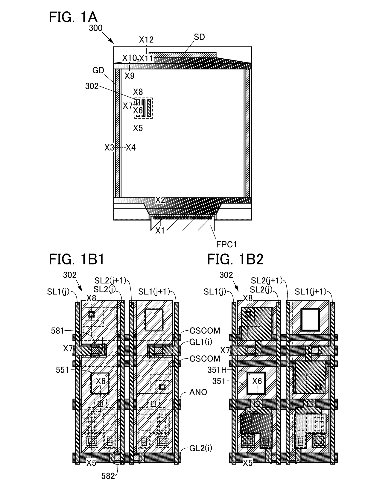
[0098]FIG. 1A is a bottom view illustrating the structure of a display device 300 of one embodiment of the present invention. FIG. 1B1 is a bottom view illustrating part of FIG. 1A. FIG. 1B2 is a bottom view omitting some components illustrated in FIG. 1B1.

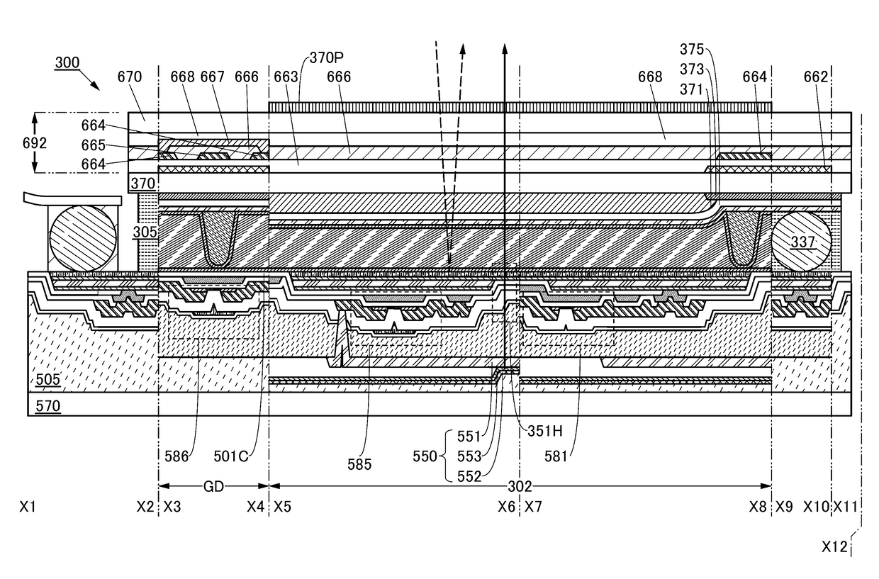
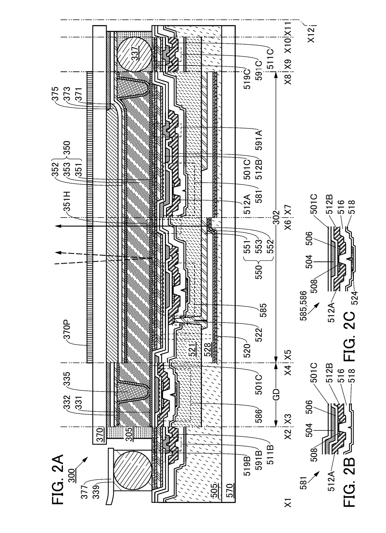
[0099]FIGS. 2A, 2B, and 2C are cross-sectional views illustrating the structure of the display device 300 of one embodiment of the present invention. FIG. 2A is a cross-sectional view taken along dashed-dotted lines X1-X2, X3-X4, X5-X6, X7-X8, X9-X10, and X11-X12 in FIG. 1A. FIG. 2B is a cross-sectional view illustrating part of the display device. FIG. 2C is a cross-sectional view illustrating other part of the display device.

[0100]FIG. 3 illustrates a circuit of a pixel 302 included in the display device 300 of one embodiment of the present invention.

[0101]As illustrated in FIG. 1A, the display ...

embodiment 2

[0447]In this embodiment, a transistor which can be used in a display device of one embodiment of the present invention is described with reference to FIGS. 20 to 34.

[0448]FIG. 20A is a top view of a transistor 200 that can be used in a display device of one embodiment of the present invention. FIG. 20B is a cross-sectional view taken along a dashed-dotted line X1-X2 in FIG. 20A. FIG. 20C is a cross-sectional view taken along a dashed-dotted line Y1-Y2 in FIG. 20A. Note that in FIG. 20A, some components of the transistor 200 (e.g., an insulating film serving as a gate insulating film) are not illustrated to avoid complexity. Furthermore, the direction of the dashed-dotted line X1-X2 may be referred to as a channel length direction, and the direction of the dashed-dotted line Y1-Y2 may be referred to as a channel width direction. As in FIG. 20A, some components are not illustrated in some cases in top views of transistors described below.

[0449]The transistor 200 includes a conductive...

embodiment 3

[0636]In this embodiment, the structure and the like of an oxide semiconductor will be described with reference to FIGS. 35 to 39.

[0637]An oxide semiconductor is classified into a single crystal oxide semiconductor and a non-single-crystal oxide semiconductor. Examples of a non-single-crystal oxide semiconductor include a c-axis-aligned crystalline oxide semiconductor (CAAC-OS), a polycrystalline oxide semiconductor, a nanocrystalline oxide semiconductor (nc-OS), an amorphous-like oxide semiconductor (a-like OS), and an amorphous oxide semiconductor.

[0638]From another perspective, an oxide semiconductor is classified into an amorphous oxide semiconductor and a crystalline oxide semiconductor. Examples of a crystalline oxide semiconductor include a single crystal oxide semiconductor, a CAAC-OS, a polycrystalline oxide semiconductor, and an nc-OS.

[0639]An amorphous structure is generally thought to be isotropic and have no non-uniform structure, to be metastable and not have fixed pos...


PUM


Abstract

Provided is a novel display device which is highly convenient and reliable. The display device includes a first display element, a second display element, and a pixel circuit. The first display element includes a first electrode and a liquid crystal layer. The second display element includes a second electrode and a light-emitting layer. The first electrode includes a reflective film. The reflective film includes an opening. The first electrode and the second electrode are electrically connected to the pixel circuit. The light-emitting layer includes a quantum dot. The second display element is configured emit light toward the opening. The first display element and the second display element are configured to perform display in the same direction.

Description

BACKGROUND OF THE INVENTION[0001]1. Field of the Invention[0002]One embodiment of the present invention relates to a display device and a manufacturing method thereof.[0003]Note that one embodiment of the present invention is not limited to the technical field. The technical field of one embodiment of the invention disclosed in this specification and the like relates to an object, a method, or a manufacturing method. One embodiment of the present invention relates to a process, a machine, manufacture, and a composition of matter. Specifically, examples of the technical field of one embodiment of the present invention disclosed in this specification include a semiconductor device, a display device, a liquid crystal display device, a light-emitting device, a lighting device, a power storage device, a memory device, a method for driving any of them, and a method for manufacturing any of them.[0004]2. Description of the Related Art[0005]There is a liquid crystal display device in which ...

Claims


Application Information

Patent Timeline
Patent Type & Authority Applications(United States)
IPC IPC(8): G02F1/1335H01L51/50H01L27/12
CPCG02F1/133603H01L27/1225H01L51/502G02F2001/133614H01L51/5056G02F1/133553H01L51/5088B82Y20/00G02F1/133617G02F2201/44G02F2202/36G02F2203/09G02F1/13338G02F1/1362G02F1/133555G02F1/133614H10K59/50H10K59/40H10K59/12H10K50/115H10K50/15H10K50/17
Inventor SEO, SATOSHIHIRAKATA, YOSHIHARU
Owner SEMICON ENERGY LAB CO LTD
Why Eureka
Try Eureka