

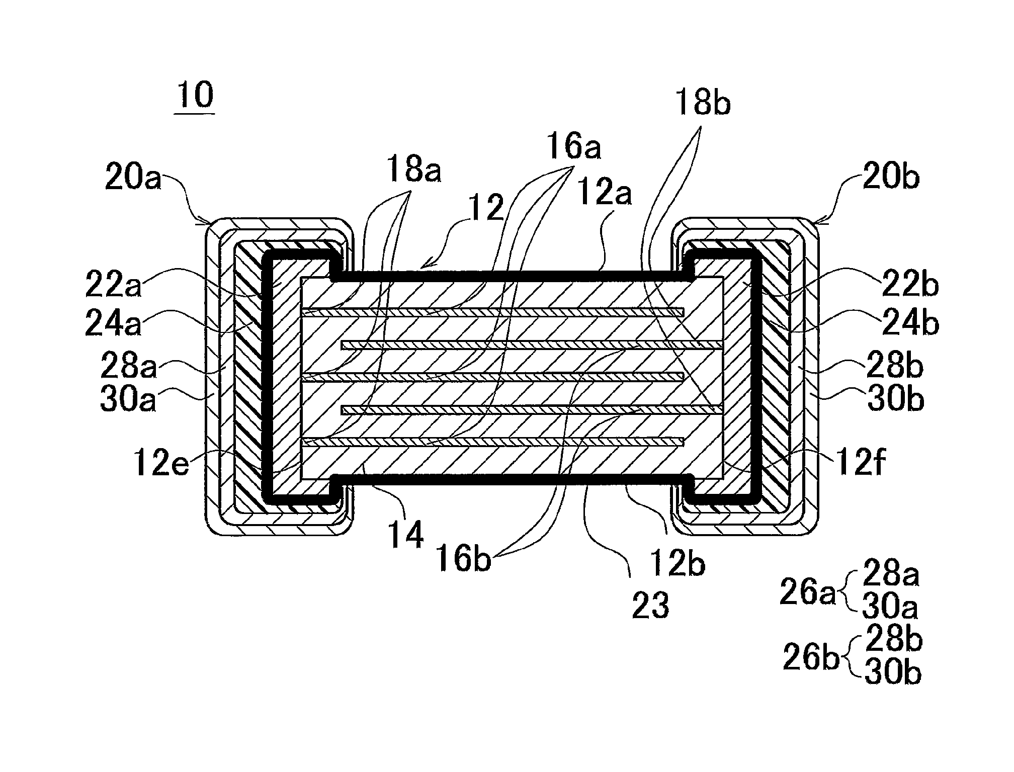
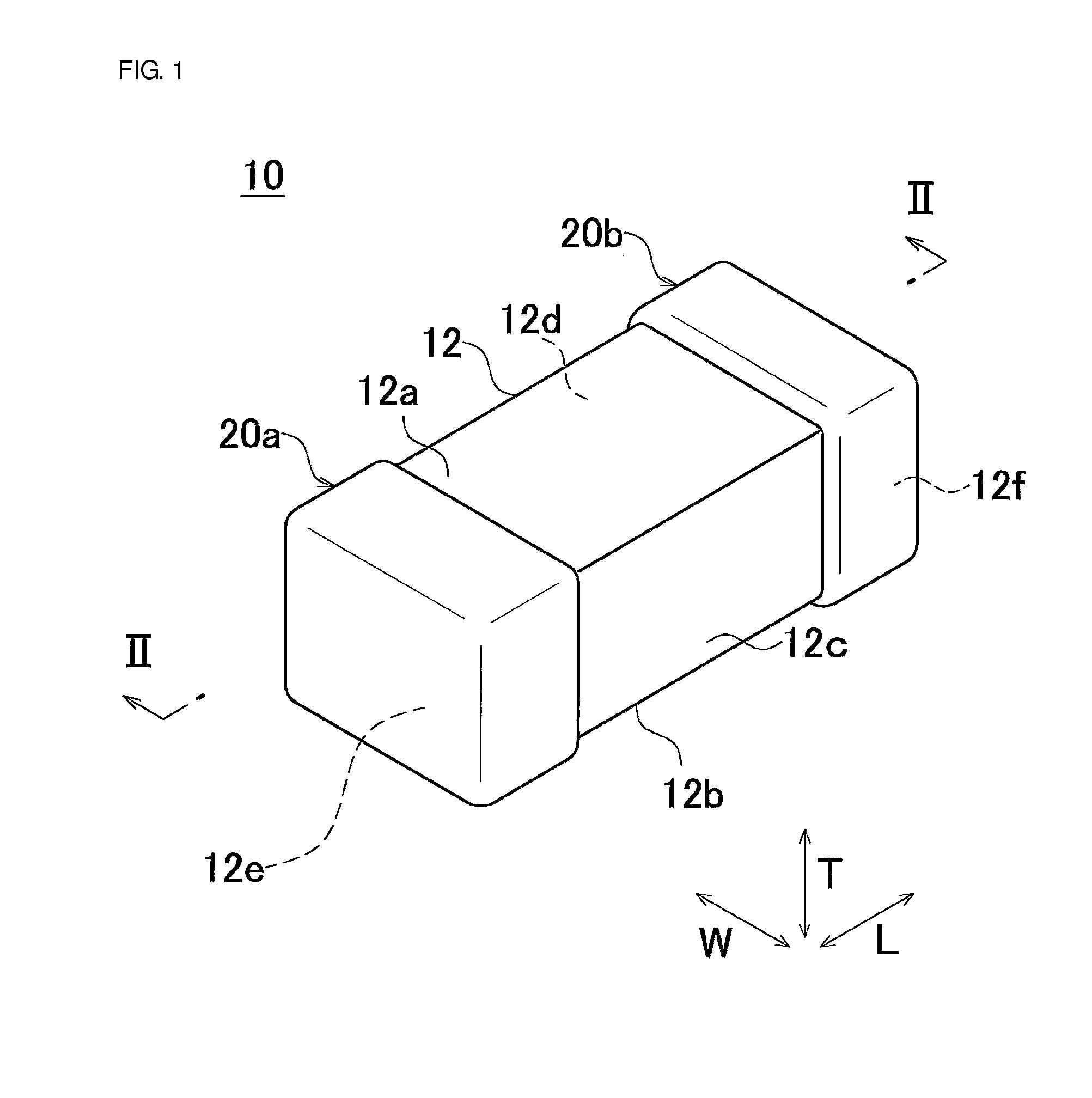
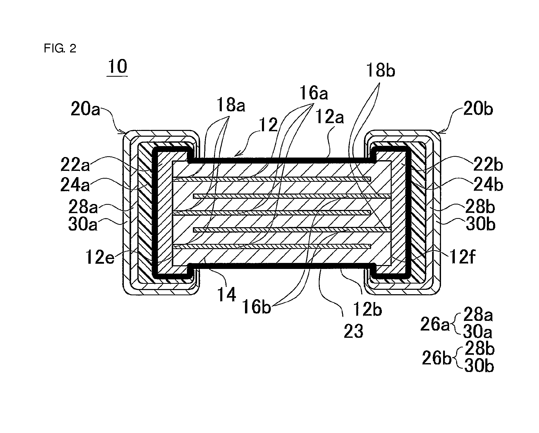
Multilayer ceramic electronic component
a ceramic electronic component and multi-layer technology, applied in the direction of fixed capacitor details, generator/motor, fixed capacitors, etc., can solve the problems of low resistance to deformation of substrates, easy cracks in ceramic base bodies, and easy ingress of moisture into the interface between the main surface of ceramic base bodies and the edge portion of outer electrodes, so as to prevent solder splatter
- Summary
- Abstract
- Description
- Claims
- Application Information
AI Technical Summary
Benefits of technology
Problems solved by technology
Method used
Image

Examples
examples
[0068]First, twenty multilayer ceramic capacitors having a fluorine layer between a ceramic base body and a sintered metal layer and twenty multilayer ceramic capacitors having a fluorine layer between a sintered metal layer and a conductive resin layer were prepared as Examples.
[0069]Furthermore, twenty multilayer ceramic capacitors having no fluorine layers were prepared as Comparative Examples.
[0070]Each of these multilayer ceramic capacitors was soldered to a substrate by reflow. As a result, in Comparative Examples, ingress of moisture into the conductive resin layers was observed, and fifteen out of twenty capacitors caused solder splatter. On the other hand, in Examples, solder splatter did not occur.
[0071]In the above-described preferred embodiments and Examples, each of the first and second outer electrodes has its edge portions disposed on the main surfaces and side surfaces of the ceramic base body. However, the side surfaces of the ceramic base body do not need to have t...
PUM
| Property | Measurement | Unit |
|---|---|---|
| thickness | aaaaa | aaaaa |
| thickness | aaaaa | aaaaa |
| thickness | aaaaa | aaaaa |
Abstract
Description
Claims
Application Information