

Semiconductor device and fabrication method thereof
a technology of semiconductors and semiconductors, applied in the direction of basic electric elements, electrolysis processes, electrolysis components, etc., can solve the problems of reduced size of integrated circuit devices, decreased performance of metal interconnect structures formed in each dielectric layer, and decreased manufacturing process nodes of traditional ic manufacturing processes
- Summary
- Abstract
- Description
- Claims
- Application Information
AI Technical Summary
Benefits of technology
Problems solved by technology
Method used
Image

Examples
Embodiment Construction
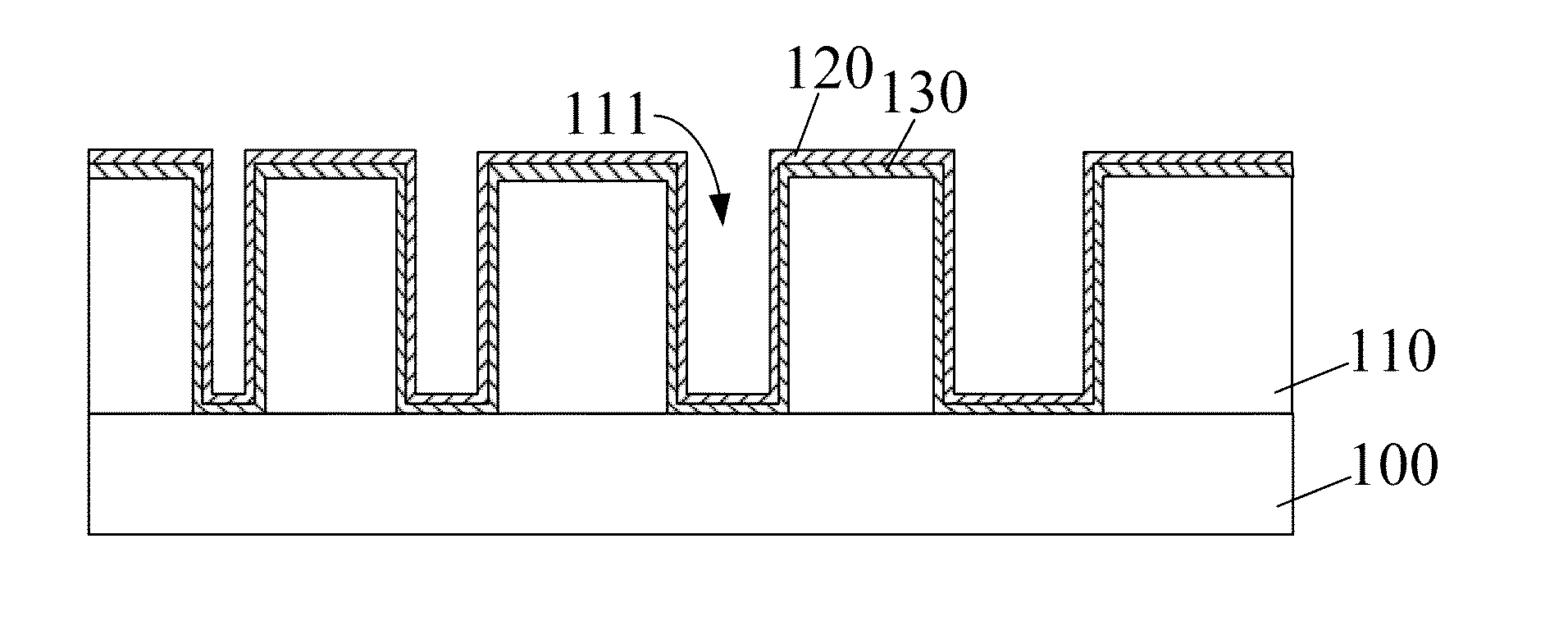
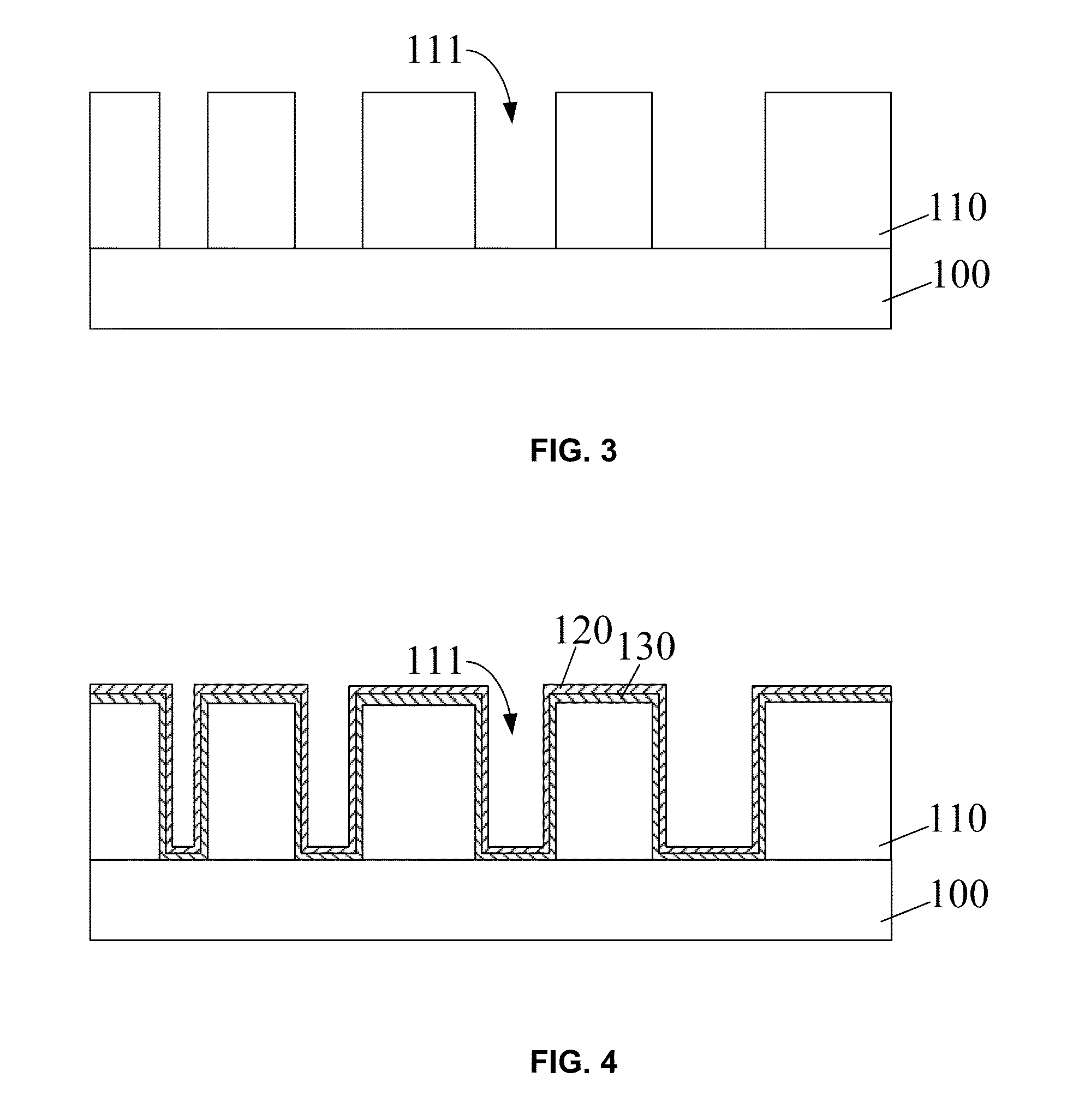
[0017]Reference will now be made in detail to exemplary embodiments of the invention, which are illustrated in the accompanying drawings. Hereinafter, embodiments consistent with the disclosure will be described with reference to drawings. Wherever possible, the same reference numbers will be used throughout the drawings to refer to the same or like parts. It is apparent that the described embodiments are some but not all of the embodiments of the present invention. Based on the disclosed embodiments, persons of ordinary skill in the art may derive other embodiments consistent with the present disclosure, all of which are within the scope of the present invention.
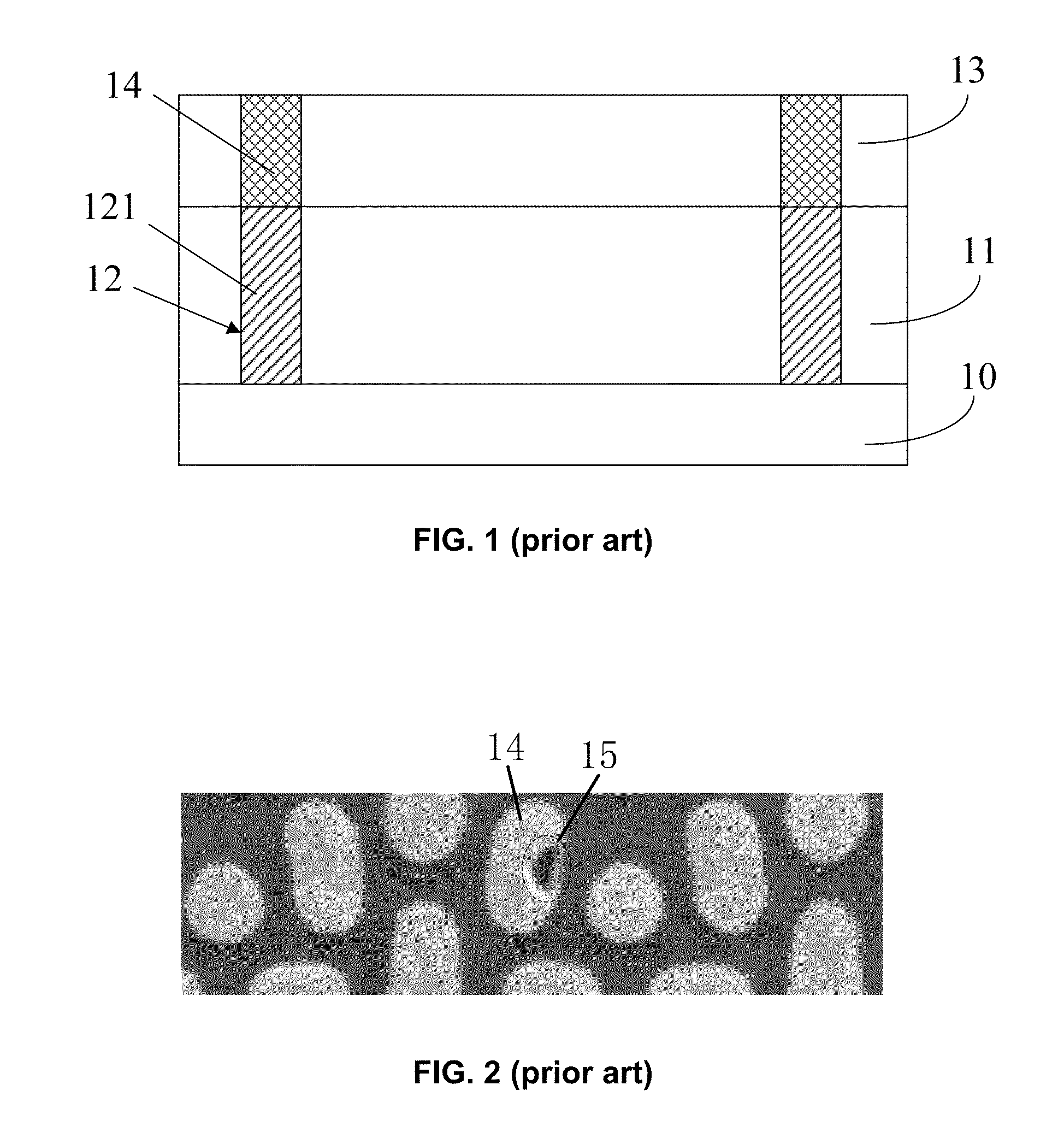
[0018]FIG. 2 is a SEM image of a conductive plug formed using a conventional fabrication process. In FIG. 2, a large number of voids 15 can be seen in a conventional conductive plug. In the life span of the semiconductor device, the subsequently formed conductive plugs may be disconnected, have high resistance and / or electr...
PUM
 Abstract
Description
Claims
Application Information