Pattern generators employing processors to vary delivery dose of writing beams according to photoresist thickness, and associated methods

a pattern generator and writing beam technology, applied in the field of microlithography patterning, can solve the problems of difficult to achieve the same photoresist thickness uniformly across the substrate, difficult effective spin coating of photoresist, and non-uniform feature size, and achieve the effect of precise critical dimensional control of pattern features and predictable performance characteristics

Active Publication Date: 2016-07-28
APPLIED MATERIALS INC
View PDF1 Cites 7 Cited by
  • Summary
  • Abstract
  • Description
  • Claims
  • Application Information

AI Technical Summary

Benefits of technology

[0008]In one embodiment a multi-beam pattern generator is disclosed. The pattern generator may include a stage configured to support a substrate in a plurality of writing cycle zone locations during respective ones of a plurality of writing cycles. The pattern generator may also include a writing beam actuator to independently direct each of a plurality of writing beams to writing pixel locations disposed upon a photoresist of the substrate. The pattern generator may also include a computer processor to adjust the delivered pixel dose for the respective writing pixel positions according to a thickness of the photoresist at the respective writing pixel locations. In this manner, more precise critical dimensional control of pattern features may be obtained on substrates with photoresist thickness variation.
[0009]In another embodiment, a method of writing a pattern with a multi-beam pattern generator is disclosed. The method may include supporting a substrate with a stage in a plurality of writing cycle zone locations during respective ones of a plurality of writing cycles. The method may also include instructing, with a computer processor, a writing beam actuator to independently direct a plurality of writing beams to writing pixel locations disposed upon a photoresist of the substrate. The method may also include adjusting writing pixel doses delivered to the writing pixel locations according to a thickness of the photoresist at a portion of the substrate. In this manner, resulting electrical devices formed with the pattern on the substrate may have more predictable performance characteristics.

Problems solved by technology

However, in the case of large rectangular-shaped substrates, it is more difficult to achieve the same photoresist thickness uniformly across the substrate.
Indeed, substrates for flat panel display manufacturing are in some cases sixteen (16) times larger than those substrates used in wafer microlithography and have a non-circular shape which makes effective spin coating of photoresist difficult.
This non-uniformity of feature size may negatively impact the performance of electronic devices formed by the pattern features, whether the substrate is intended to support flat panel display manufacturing or other electronic-based products.

Method used


Image

  • Pattern generators employing processors to vary delivery dose of writing beams according to photoresist thickness, and associated methods
  • Pattern generators employing processors to vary delivery dose of writing beams according to photoresist thickness, and associated methods
  • Pattern generators employing processors to vary delivery dose of writing beams according to photoresist thickness, and associated methods

Examples


fourth embodiment

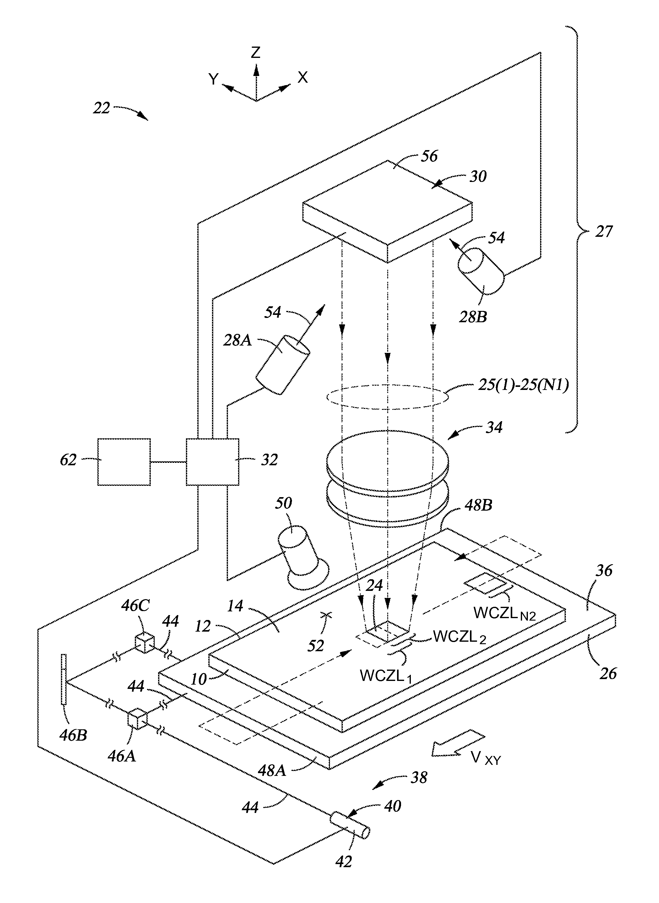
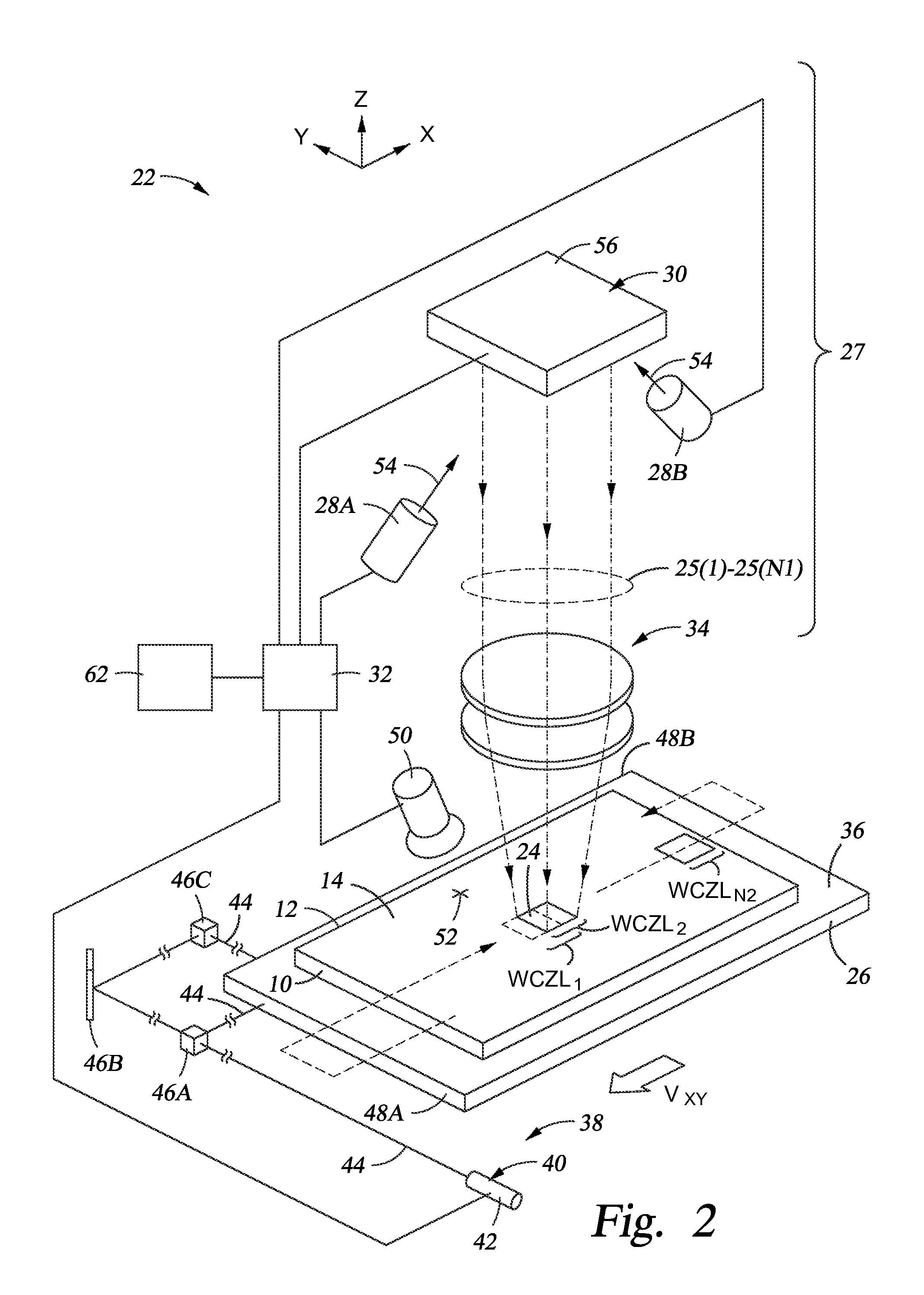
[0080]In one case of this embodiment as illustrated in FIG. 12B, during the writing cycles WC5, WC6 the computer processor 32 provides instruction so that the frequency of the pulses of the light 56 may increase to a frequency of ten (10) pulses per writing cycle from the nominal frequency of eight (8) pulses per writing cycles as instructed in writing cycles WC1 through WC4. The higher frequency compensates for the thicker resist thickness TH1 as shown in FIG. 12D. In writing cycle WCN2, the computer processor 32 instructs the frequency of the pulse of the light 56 to decrease to seven (7) pulses per writing cycle from a nominal eight (8) pulses to compensate for the thinner resist thickness TH2. In this manner, changing the frequency of the pulses of the light 56 may be used to compensate for deviations in photoresist thickness and achieve higher uniformity. It is understood that a combination of the third and fourth embodiment may also be used.

fifth embodiment

[0081]A fifth embodiment is also disclosed. In this regard, a portion 208 of the mirrors 58(1)-58(N1) may be turned off adjust a cumulated dose delivered to a pattern feature in order to compensate for deviation thickness of the photoresist. In this regard, FIGS. 13A through 13F are schematic drawings of the SLM 56 superimposed upon the substrate 10 in six (6) respective writing cycle zone locations, respectively. A photoresist section 14A attached to the substrate 10 may include a thickness which is thinner than a thickness of a photoresist section 14B attached to the substrate 10. Accordingly, a dose adjustment may be used to improve uniformity of feature sizes. As depicted in FIG. 13A, a first feature 210A and a second feature 210B of the pattern to be written may be disposed in the photoresist sections 14A, 14B, respectively. As the mirrors 58(1)-58(N1) and the substrate 10 move relative to each other cumulative pixel doses are applied to write the first feature 210A and the sec...


PUM

PropertyMeasurementUnit
thicknessaaaaaaaaaa
widthaaaaaaaaaa
widthaaaaaaaaaa

Abstract

Multi-beam pattern generators employing processors to vary delivered dose of writing beams according to photoresist thicknesses, and associated methods are disclosed. A pattern generator may write a pattern upon a substrate having a photoresist which is sensitive to the writing beams. The pattern may be written in respective writing cycles when the writing beams write at least a portion of the pattern at writing pixel locations. A beam actuator of the pattern generator may independently direct the writing beams to the writing pixels to deliver respective pixel doses during each writing cycle. Pixel doses delivered may be adjusted according to a thickness of the photoresist at various writing pixel locations according to one or more approaches, using one or more of: actuator dwell times, emitted pulse duration, emitted pulse frequency, and emitted pulse intensity. In this manner, additional dimensional control is provided for substrates having variable photoresist thicknesses.

Description

BACKGROUND[0001]1. Field[0002]Embodiments of the present disclosure generally relate to apparatuses and methods for microlithography patterning and more particularly for microlithography patterning for large substrates with a photoresist film applied.[0003]2. Description of the Related Art[0004]Large area substrates are often utilized to support electrical features used in electronic devices. In some cases, large area substrates are used when manufacturing flat panels for active matrix displays such as computers, touch panel devices, personal digital assistances (PDAs), cell phones, television monitors, and the like. Generally, flat panels may comprise a layer of liquid crystal material forming pixels sandwiched between two plates. When power from the power supply is applied across the liquid crystal material during use, an amount of light passing through the liquid crystal material may be precisely controlled at pixel locations enabling images to be generated.[0005]In some cases, m...

Claims


Application Information

Patent Timeline
Patent Type & Authority Applications(United States)
IPC IPC(8): G03F7/20
CPCG03F7/702G03F7/70558G03F7/70383G03F7/70608G03F7/2059G03F7/70041G03F7/7055
Inventor BENCHER, CHRISTOPHER DENNIS
Owner APPLIED MATERIALS INC
Why Eureka
Try Eureka