Eureka AIR delivers breakthrough ideas for toughest innovation challenges, trusted by R&D personnel around the world.

Memory device and operation method thereof

Active Publication Date: 2016-10-06
SK HYNIX INC
View PDF3 Cites 2 Cited by
  • Summary
  • Abstract
  • Description
  • Claims
  • Application Information

AI Technical Summary

Benefits of technology

The invention is about improving the security of a memory device by using a data erasure circuit to protect against unauthorized access. The technology allows for the memory device to switch between different interfaces and modes to input and output data. The interface chip can also erase the data on the memory chips if the mode switches between them. This helps to ensure that the data is always secure and safe.

Problems solved by technology

However, there may data security issues where data of the host apparatus is lost through the other interface.

Method used


Image

  • Memory device and operation method thereof
  • Memory device and operation method thereof
  • Memory device and operation method thereof

Examples


Embodiment Construction

[0016]Various embodiments will be described below in more detail with reference to the accompanying drawings. The present invention may, however, be embodied in different forms and should not be construed as limited to the embodiments set forth herein. Rather, these embodiments are provided so that this disclosure will be thorough and complete, and will fully convey the scope of the present invention to those skilled in the art. Throughout the disclosure, like reference numerals refer to like parts throughout the various figures and embodiments of the present invention.

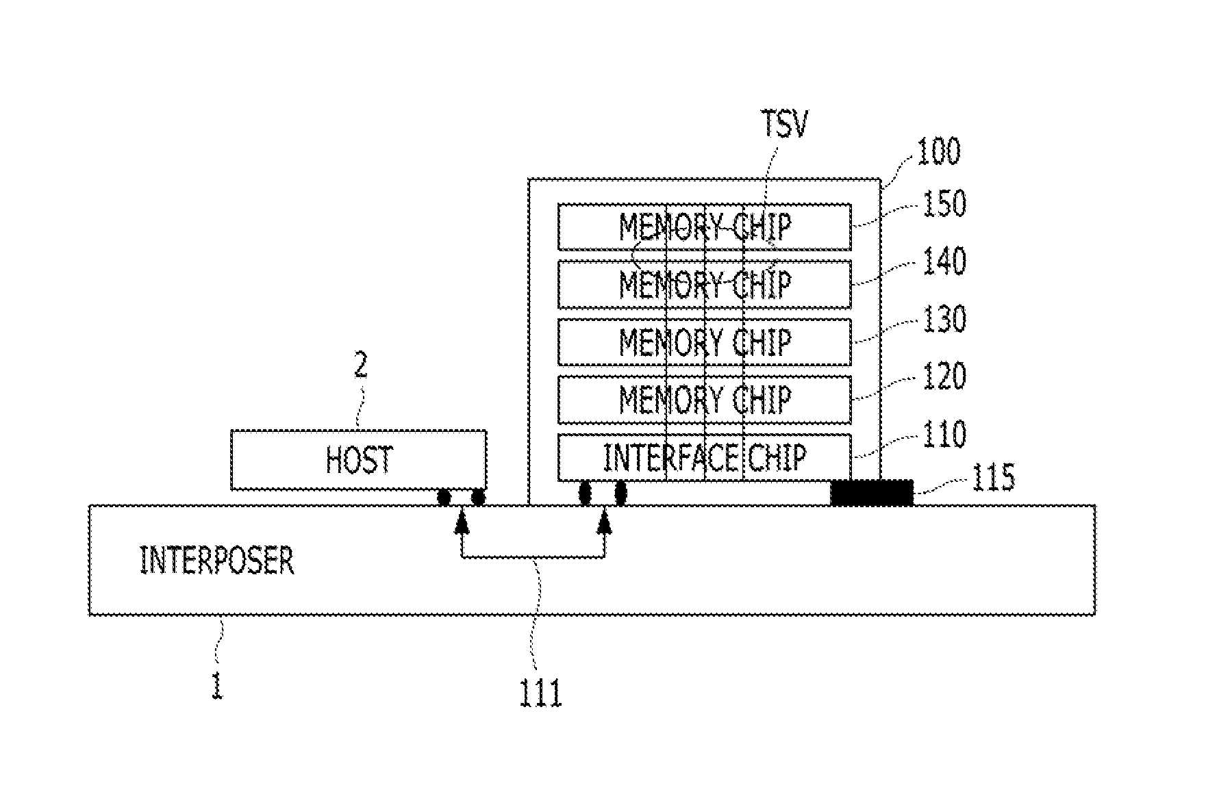
[0017]FIG. 1 is a diagram illustrating a memory device 100 in accordance with an embodiment of the present invention.

[0018]Referring to FIG. 1, the memory device 100 may include a plurality of stacked chips 110˜150. An interface chip 110 may be provided at the bottom of the memory device 100 and memory chips 120˜150 may be stacked over the interface chip 110. Each of the memory chips 120˜150 may include a cell array. ...


PUM


Abstract

A memory device may include a plurality of cell arrays, a first interface suitable for inputting / outputting first data between the plurality of cell arrays and a host apparatus, a second interface suitable for inputting / outputting second data between the plurality of cell arrays and a device other than the host apparatus, and a data erasure circuit suitable for erasing the first data of the plurality of cell arrays when a first mode in which the first interface is used switches to a second mode in which the second interface is used.

Description

CROSS-REFERENCE TO RELATED APPLICATION[0001]The present application claims priority of Korean Patent Application No. 10-2015-0048445, filed on Apr. 6, 2015, which is incorporated herein by reference in its entirety.BACKGROUND[0002]1. Field[0003]Exemplary embodiments of the present invention relate to a memory device and, more particularly, to a technology for improving the data security of a memory device.[0004]2. Description of the Related Art[0005]In most electronic systems, semiconductor memory devices are used as a storage device. Semiconductor memory devices are being developed to increase not only their data storage capacities but also their data processing speeds. Furthermore, various attempts to mount memory devices of higher capacity within a smaller area and to efficiently drive the memory devices are being made.[0006]In order to improve memory device integration, two-dimensional (2D) arrangement methods have been supplanted by three-dimensional (3D) arrangement methods in...

Claims


Application Information

Patent Timeline
IPC IPC(8): G11C7/10
CPCG11C7/10G11C5/04G11C7/1045G11C7/20G11C29/36G11C2029/0401
Inventor KIM, DAE-SUK
Owner SK HYNIX INC
Why Eureka
Eureka Blog
Learn More