Capacitor With 3D NAND Memory

a technology of nand memory and capacitors, applied in capacitors, diodes, semiconductor devices, etc., can solve the problems of increasing complexity and cost of the overall integrated circuit, and the limitations of the conventional integrated circuit to relatively small capacitors

Active Publication Date: 2017-01-19
MACRONIX INT CO LTD
View PDF5 Cites 292 Cited by
  • Summary
  • Abstract
  • Description
  • Claims
  • Application Information

AI Technical Summary

Problems solved by technology

While providing capacitors of various sizes is usually not a problem outside of an integrated circuit, conventional integrated circuits are limited to relatively small capacitors because of size limitations.
However, the stacked capacitor is fabricated by many steps which results in increased complexity and cost of the overall integrated circuit.

Method used


Image

  • Capacitor With 3D NAND Memory
  • Capacitor With 3D NAND Memory
  • Capacitor With 3D NAND Memory

Examples


Embodiment Construction

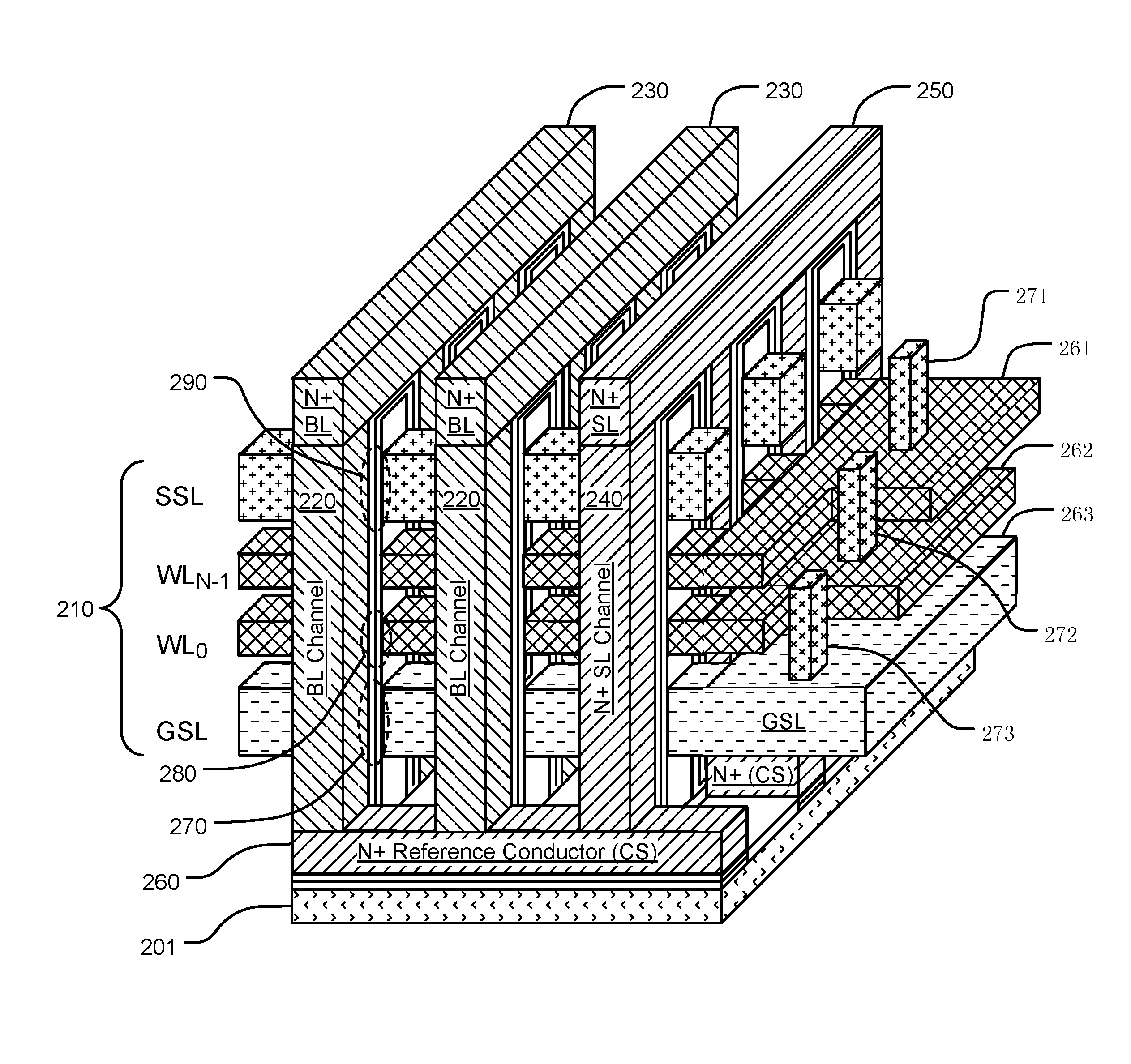
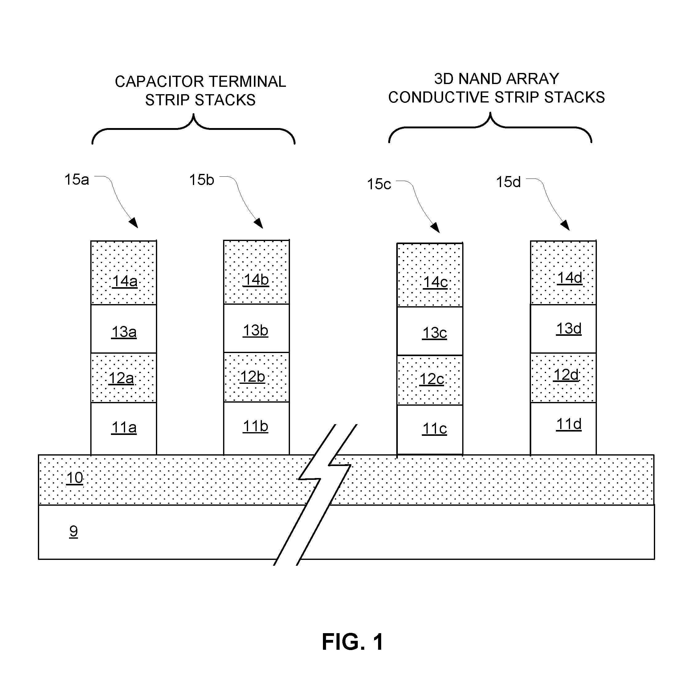
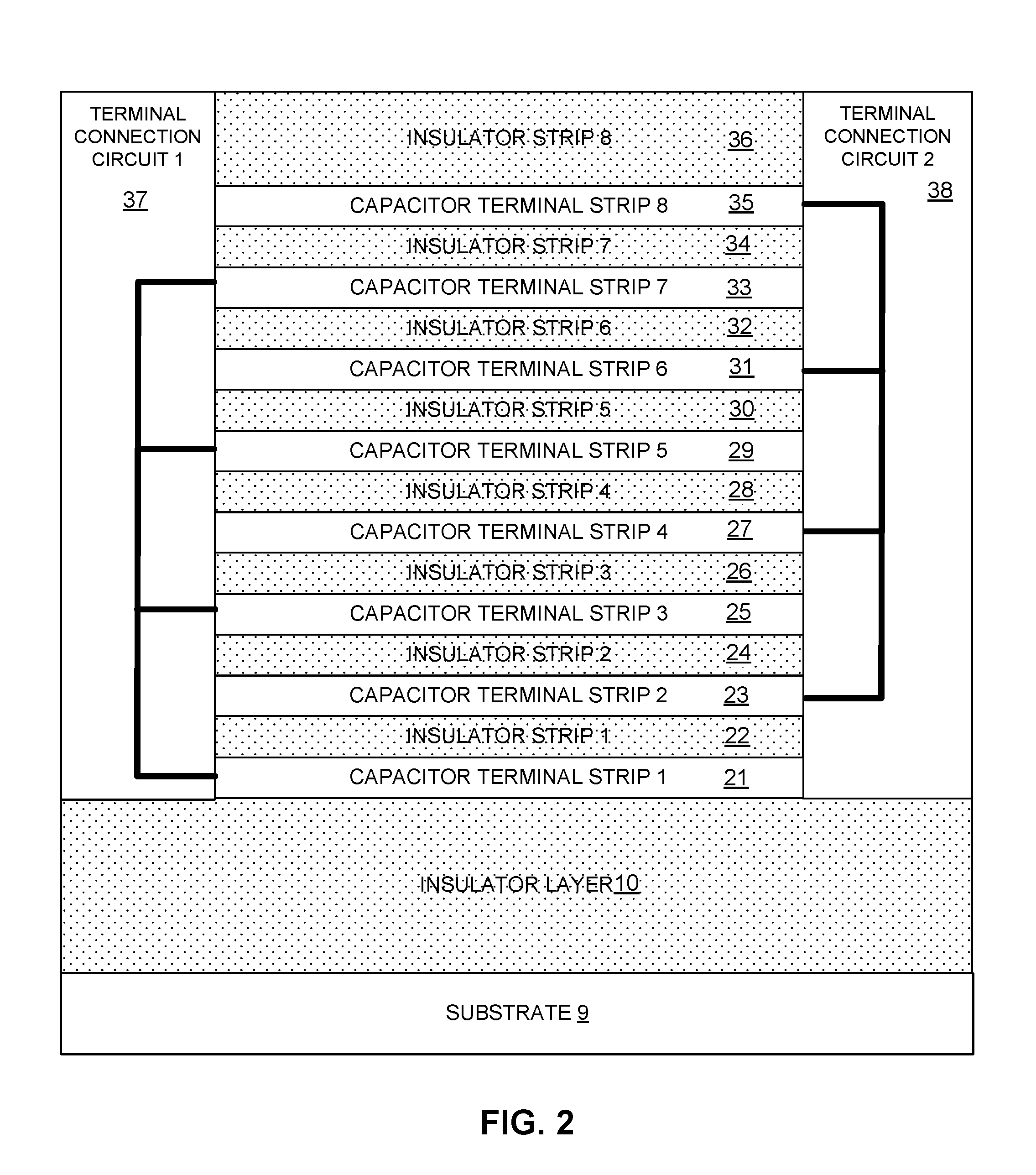
[0027]The following description will typically be with reference to specific structural embodiments and methods. It is to be understood that there is no intention to limit the invention to the specifically disclosed embodiments and methods but that the invention may be practiced using other features, elements, methods and embodiments. Preferred embodiments are described to illustrate the present invention, not to limit its scope, which is defined by the claims. Those of ordinary skill in the art will recognize a variety of equivalent variations on the description that follows. Like elements in various embodiments are commonly referred to with like reference numerals.

[0028]It is widely recognized that capacitance is very useful electronic circuitry, but is expensive and has manufacturing difficulties when manufactured in semiconductors. Capacitance can be used to help reduce voltage variations and can be used to help save data in memory, such as SRAM, DRAM and Flash, either during no...


PUM


Abstract

An integrated circuit includes a 3D NAND memory array with a stack of conductive strips and a capacitor with a stack of capacitor terminal strips. Multiple conductive strips in the stack of conductive strips, and multiple capacitor terminal strips of the stack of capacitor terminal strips, share a same plurality of plane positions relative to the substrate. Different plane positions in the same plurality of plane positions characterize different capacitor terminal strips in the stack of capacitor terminal strips and different conductive strips in the stack of conductive strips, and a same plane position characterizing both a conductive strip in the stack of conductive strips and a capacitor terminal strip in the stack of capacitor terminal strips indicates that the conductive strip and the capacitor terminal strip have a same vertical position relative to each other.

Description

CROSS-REFERENCE TO OTHER APPLICATIONS[0001]This application is a divisional of co-pending U.S. patent application Ser. No. 14 / 739,717 filed on 15 Jun. 2015; which application is related to the following co-pending U.S. patent applications: U.S. patent application Ser. No. 13 / 049,303, filed 16 Mar. 2011, entitled REDUCED NUMBER OF MASK FOR IC DEVICE WITH STACKED CONTACT LEVELS, now U.S. Pat. No. 8,598,032; and U.S. patent application Ser. No. 13 / 114,931, filed 24 May 2011, entitled MULTILAYER CONNECTION STRUCTURE AND MAKING METHOD, now U.S. Pat. No. 8,383,512.BACKGROUND OF THE INVENTION[0002]Capacitors are electronic devices including two terminals separated by insulating material. When there is a voltage difference between the two terminals, an electric field is created between the two terminals thereby storing electrical energy. The amount of electrical charge that can be stored on a capacitor per volt across the terminals is referred to as capacitance. Terminals are typically in t...

Claims


Application Information

Patent Timeline
Patent Type & Authority Applications(United States)
IPC IPC(8): H01L27/115H01L27/02H01L49/02H01L27/06
CPCH01L27/11582H01L27/0629H01L28/60H01L27/11573H01L27/0207H01L27/11556H01L28/90H10B41/50H10B41/27H10B43/50H10B43/40H10B43/27H10B41/40
Inventor LUE, HANG-TINGYEH, TENG-HAO
Owner MACRONIX INT CO LTD
Why Eureka
Try Eureka