Semiconductor device, display panel, and electronic device

a technology of display panel and semiconductor, applied in the direction of digital-analog converters, static indicating devices, instruments, etc., can solve the problems of low response speed, degraded display quality, and inability to obtain desired grayscale display, and achieve the effect of higher degree of freedom of choi

Active Publication Date: 2017-02-23
SEMICON ENERGY LAB CO LTD
View PDF6 Cites 14 Cited by
  • Summary
  • Abstract
  • Description
  • Claims
  • Application Information

AI Technical Summary

Benefits of technology

[0010]As described above, there are a variety of structures of semiconductor devices functioning as grayscale voltage generation circuits. The structures have merits and demerits, and an appropriate structure i

Problems solved by technology

Moreover, the increase in the number of switches due to a larger number of digital signal bits causes the increase in parasitic capacitance of an output portion, resulting in lower response s

Method used


Image

  • Semiconductor device, display panel, and electronic device
  • Semiconductor device, display panel, and electronic device
  • Semiconductor device, display panel, and electronic device

Examples


embodiment 1

[0051]In this embodiment, an example of a semiconductor device functioning as a grayscale voltage generation circuit will be described.

[0052]In this specification and the like, a semiconductor device generally means a device that can function by utilizing semiconductor characteristics. Thus, a driver IC composed of semiconductor elements such as transistors and a display device including the driver IC are included in the category of the semiconductor device.

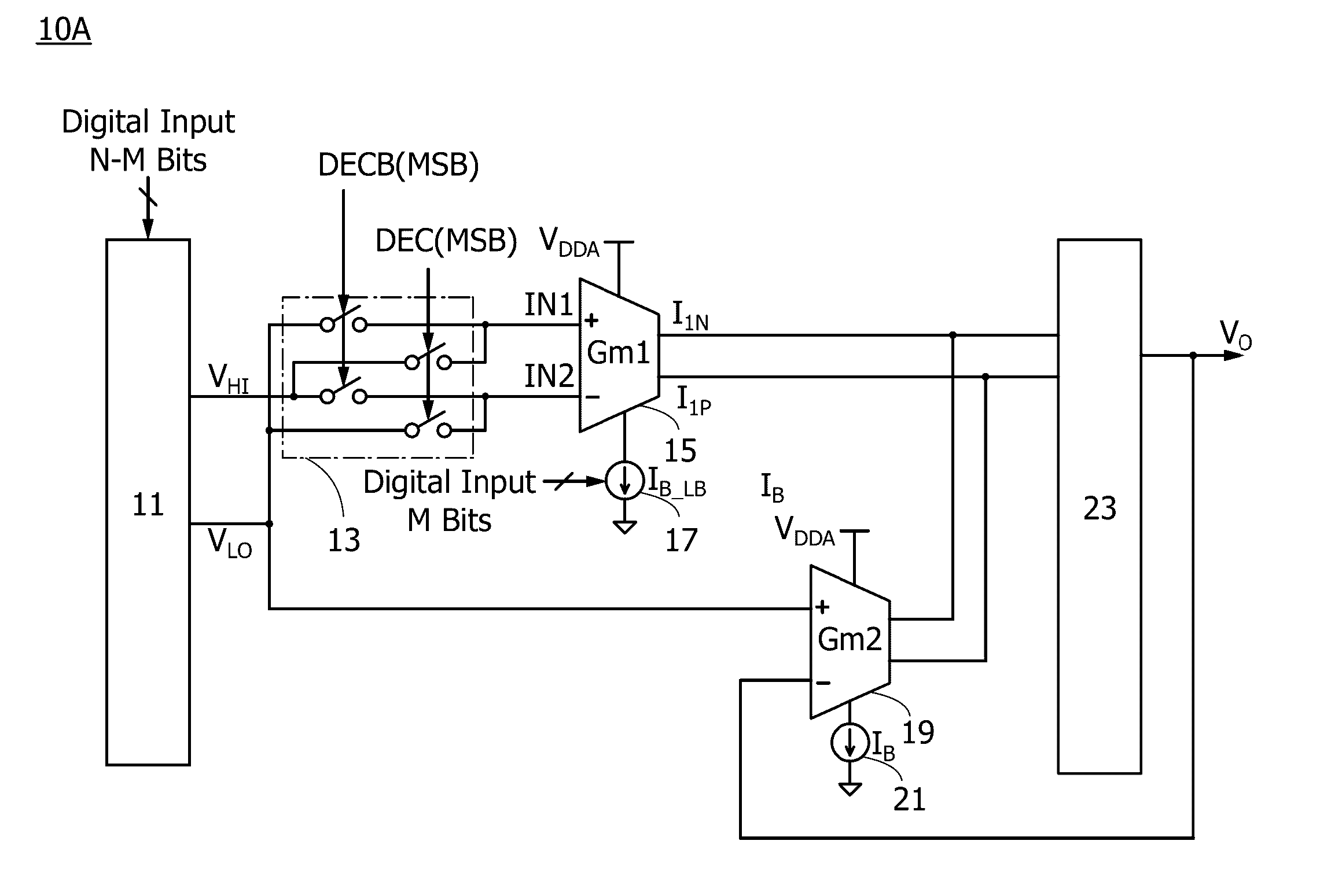
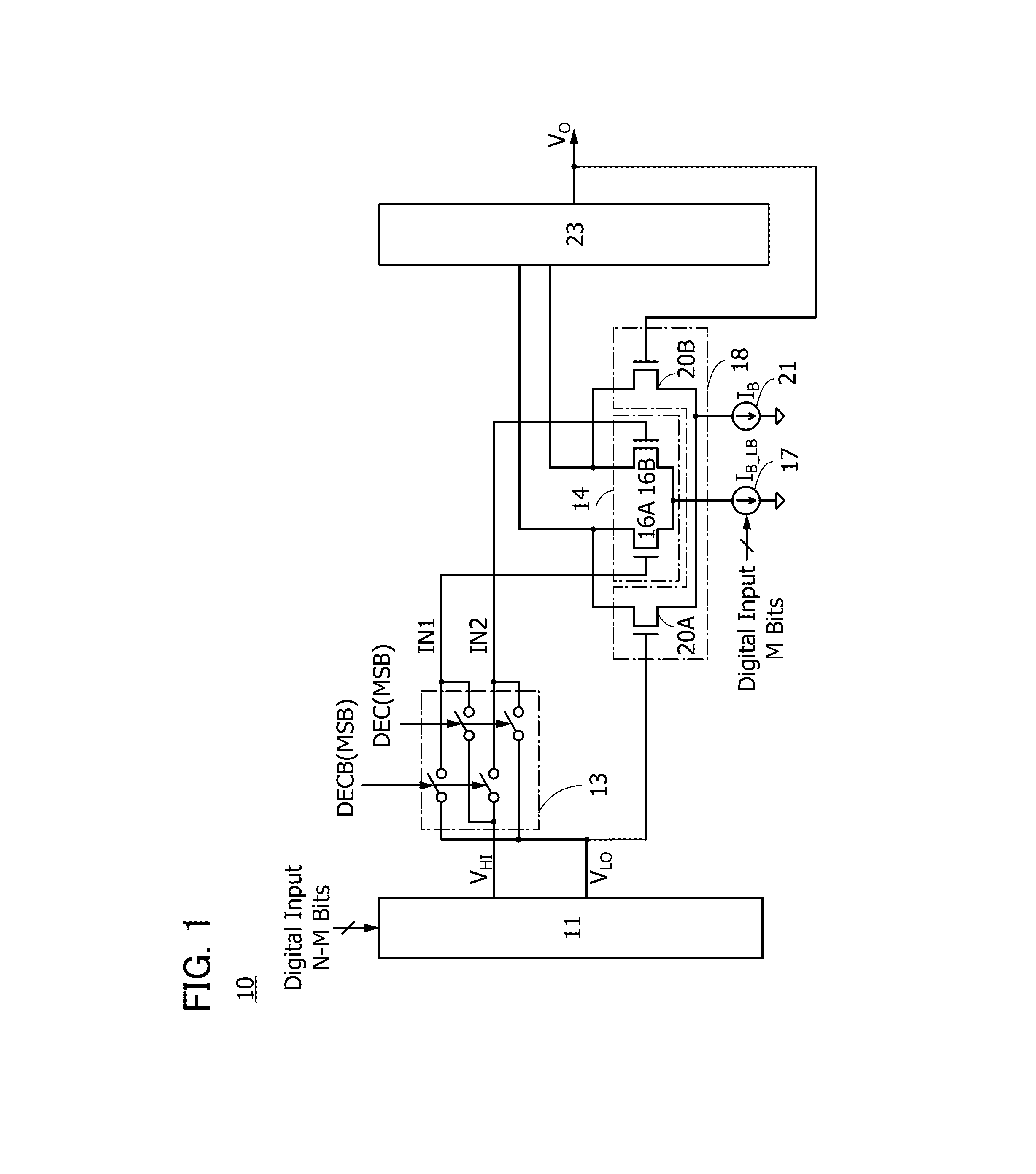
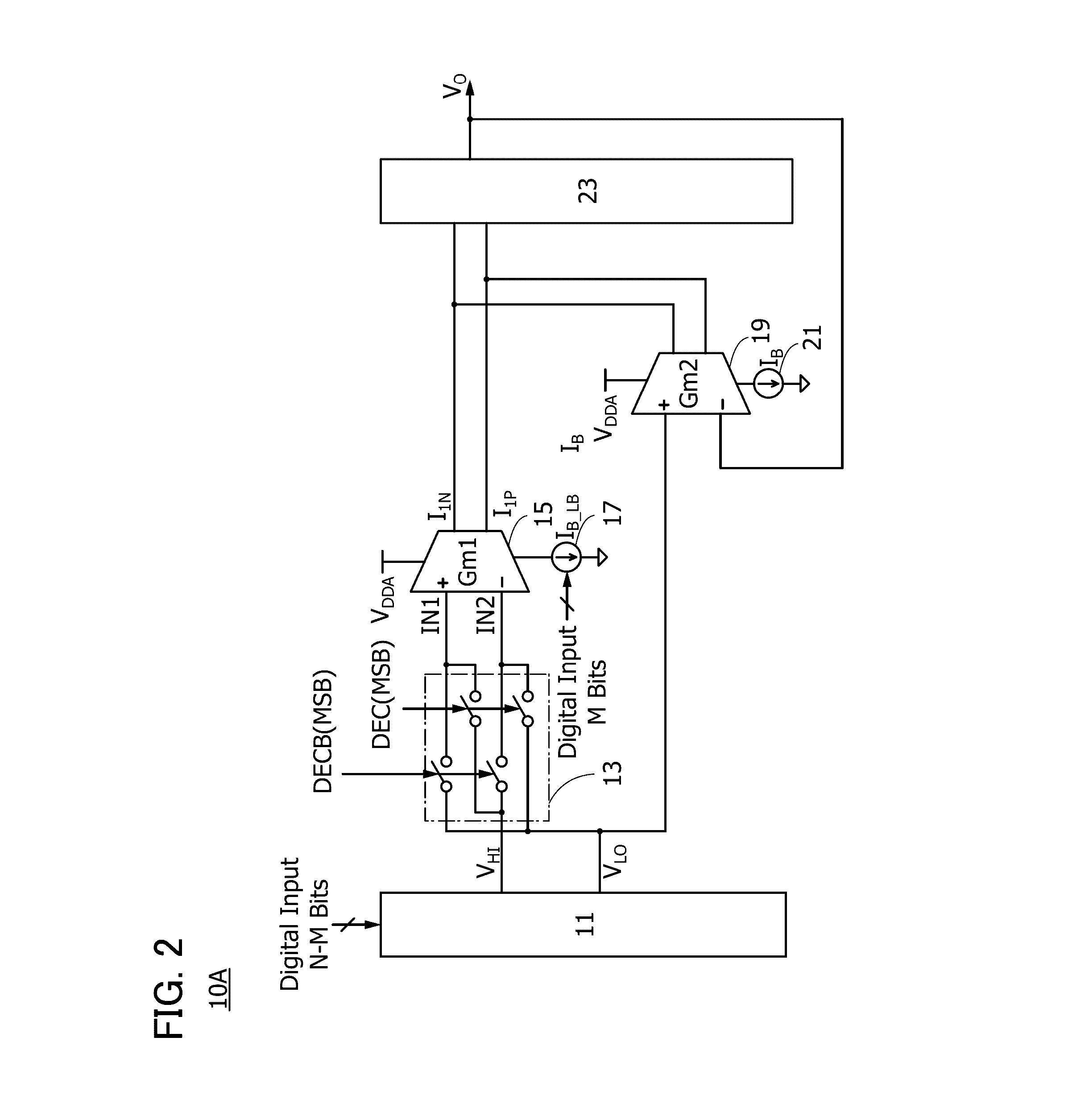
[0053]FIG. 1 is a circuit diagram illustrating an example of a circuit structure for describing a semiconductor device 10.

[0054]The semiconductor device 10 includes a digital-to-analog converter circuit (hereinafter referred to as a D / A converter circuit) 11, a differential amplifier circuit 14, a current source 17, a differential amplifier circuit 18, a current source 21, a switching circuit 13, and a current-voltage converter circuit 23.

[0055]In the case where an N-bit digital signal (N is a natural number of 2 or more) is inpu...

embodiment 2

[0108]This embodiment will explain a circuit block diagram of a display device including the semiconductor device described in Embodiment 1, which functions as a grayscale voltage generation circuit. FIG. 13 is a circuit block diagram illustrating a source driver, a gate driver, and a display portion.

[0109]The display device in the circuit block diagram of FIG. 13 includes a source driver 200, a gate driver 201, and a display portion 202. In FIG. 13, a pixel 203 is shown in the display portion 202.

[0110]The source driver 200 can include the semiconductor device described in Embodiment 1. Specifically, the source driver 200 includes a digital circuit portion 211 (denoted by Digital Block in the diagram), a D / A converter 212 (denoted by DAC in the diagram), and an output circuit portion 213 (denoted by Output Buffers in the diagram).

[0111]The source driver 200 has a function of outputting an analog signal to source lines SL[1] to SL[n] (n is a natural number of 2 or more).

[0112]The di...

embodiment 3

[0128]In this embodiment, an example of a cross-sectional structure of a semiconductor device in one embodiment of the present invention will be described with reference to FIG. 15.

[0129]The semiconductor device in the above embodiment includes the digital-to-analog converter circuit 11, the differential amplifier circuit 14, the current source 17, the differential amplifier circuit 18, the current source 21, the switching circuit 13, the current-voltage converter circuit 23, and the like and can be formed using transistors including silicon or the like. As silicon, polycrystalline silicon, microcrystalline silicon, or amorphous silicon can be used. Note that an oxide semiconductor or the like can be used instead of silicon.

[0130]FIG. 15 is a schematic cross-sectional view of a semiconductor device of one embodiment of the present invention. The semiconductor device in the schematic cross-sectional view of FIG. 15 includes an n-channel transistor and a p-channel transistor that cont...


PUM


Abstract

A semiconductor device having a novel structure is provided. Fluctuation in the grayscale voltage due to an offset voltage is suppressed. When a current corresponding to a lower-bit grayscale voltage is generated in a transconductance amplifier, voltages VHI and VLO supplied to the transconductance amplifier are alternately input to two input terminals in accordance with a digital signal of the most significant bit of lower bits. Since a change corresponding to the offset voltage is added to both the maximum and minimum values of the current output from the transconductance amplifier, fluctuation in the grayscale voltage due to the offset voltage can be suppressed.

Description

BACKGROUND OF THE INVENTION[0001]1. Field of the Invention[0002]One embodiment of the present invention relates to a semiconductor device, a display panel, and an electronic device.[0003]Note that one embodiment of the present invention is not limited to the above technical field. The technical field of the invention disclosed in this specification and the like relates to an object, a method, or a manufacturing method. In addition, one embodiment of the present invention relates to a process, a machine, manufacture, or a composition of matter. Specifically, examples of the technical field of one embodiment of the present invention disclosed in this specification include a semiconductor device, a display device, a light-emitting device, a power storage device, a memory device, a method for driving any of them, and a method for manufacturing any of them.[0004]In this specification and the like, a semiconductor device refers to an element, a circuit, a device, or the like that can func...

Claims


Application Information

Patent Timeline
IPC IPC(8): G09G3/20
CPCG09G3/2011G09G3/2096G09G2320/02G09G2310/027G09G2320/0252G09G2310/0291G09G3/3648G09G3/3688H03M1/66G09G2300/0426G09G2330/028G09G3/3283H10K19/00G09G3/20G09G3/3275G09G2300/0828
Inventor TAKAHASHI, KEI
Owner SEMICON ENERGY LAB CO LTD
Why Eureka
Try Eureka