Semiconductor device, electronic component, and electronic device

a technology of semiconductors and components, applied in the direction of digital-analog convertors, phase shifters, instruments, etc., can solve the problems of low response speed, and achieve the effect of increasing the degree of freedom of choi

Inactive Publication Date: 2016-08-18
SEMICON ENERGY LAB CO LTD
View PDF5 Cites 6 Cited by
  • Summary
  • Abstract
  • Description
  • Claims
  • Application Information

AI Technical Summary

Benefits of technology

[0012]As described above, there are a variety of structures of semiconductor devices functioning as grayscale voltage generator circuits. Each structure has advantages and disadvantages, and a structure appropriate for circumstances is selected. Thus, a proposal for a semiconductor device that has a novel structure and functions as a grayscale voltage generator circuit leads to higher degree of freedom of choice.

Problems solved by technology

Moreover, the increase in the number of switches due to a larger number of digital signal bits causes the increase in parasitic capacitance of an output portion, resulting in lower response speed.

Method used


Image

  • Semiconductor device, electronic component, and electronic device
  • Semiconductor device, electronic component, and electronic device
  • Semiconductor device, electronic component, and electronic device

Examples


embodiment 1

[0043]In this embodiment, an example of a semiconductor device functioning as a grayscale voltage generator circuit will be described.

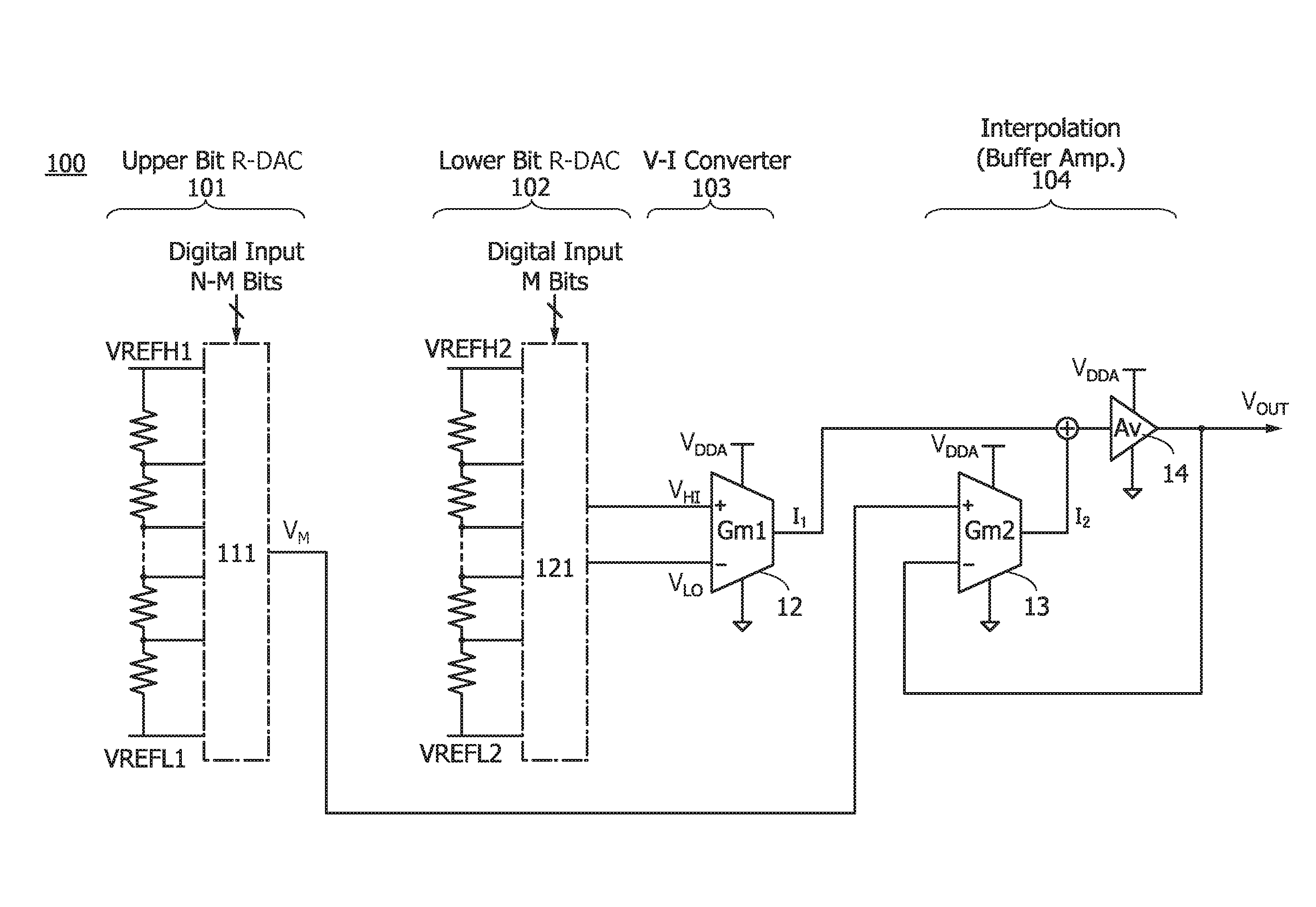
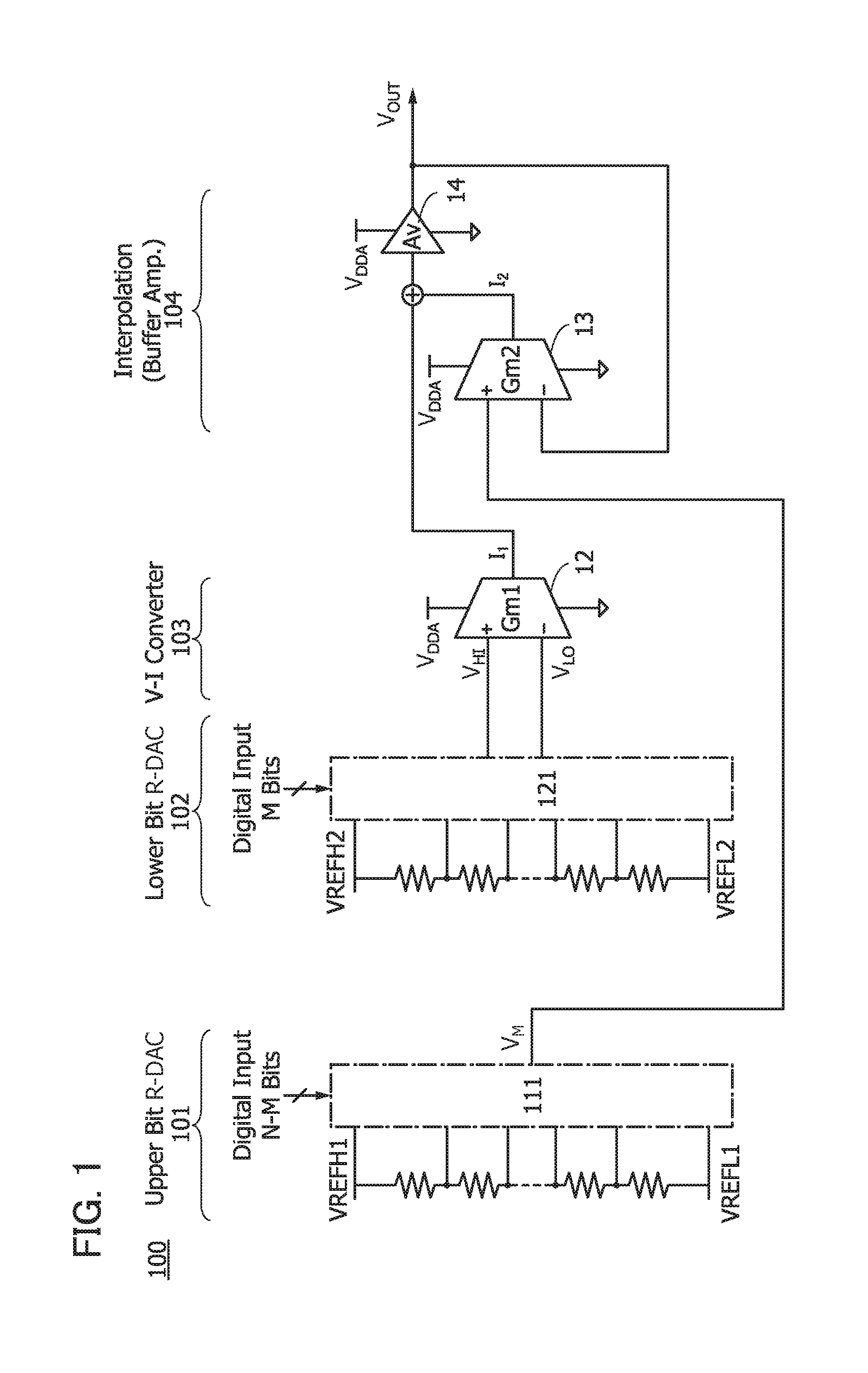
[0044]FIG. 1 is a schematic diagram showing circuit blocks of a semiconductor device 100.

[0045]The semiconductor device 100 includes a D / A converter circuit 101, a D / A converter circuit 102, a voltage-current converter circuit 103, and an interpolation circuit 104.

[0046]In the semiconductor device 100, a grayscale voltage corresponding to an upper bit of a digital signal is generated by the D / A converter circuit 101, and a grayscale voltage corresponding to a lower bit of the digital signal is generated by the D / A converter circuit 102. After the upper-bit grayscale voltage and the lower-bit grayscale voltage are generated separately, currents are generated in the voltage-current converter circuit 103 and the interpolation circuit 104 on the basis of the respective grayscale voltages. Then, these currents are synthesized in the interpolation circuit 1...

embodiment 2

[0086]This embodiment will explain a circuit block diagram of a display device including the semiconductor device described in Embodiment 1, which functions as a grayscale voltage generator circuit. FIG. 9 is a circuit block diagram illustrating a source driver, a gate driver, and a display portion.

[0087]The display device in the circuit block diagram of FIG. 9 includes a source driver 200, a gate driver 201, and a display portion 202. In FIG. 9, a pixel 203 is shown in the display portion 202.

[0088]Digital signals DATA[1] to DATA[N] (DATA[1:N] in FIG. 9) are input to a decoder DEC. The decoder DEC outputs a digital signal to the semiconductor device 100.

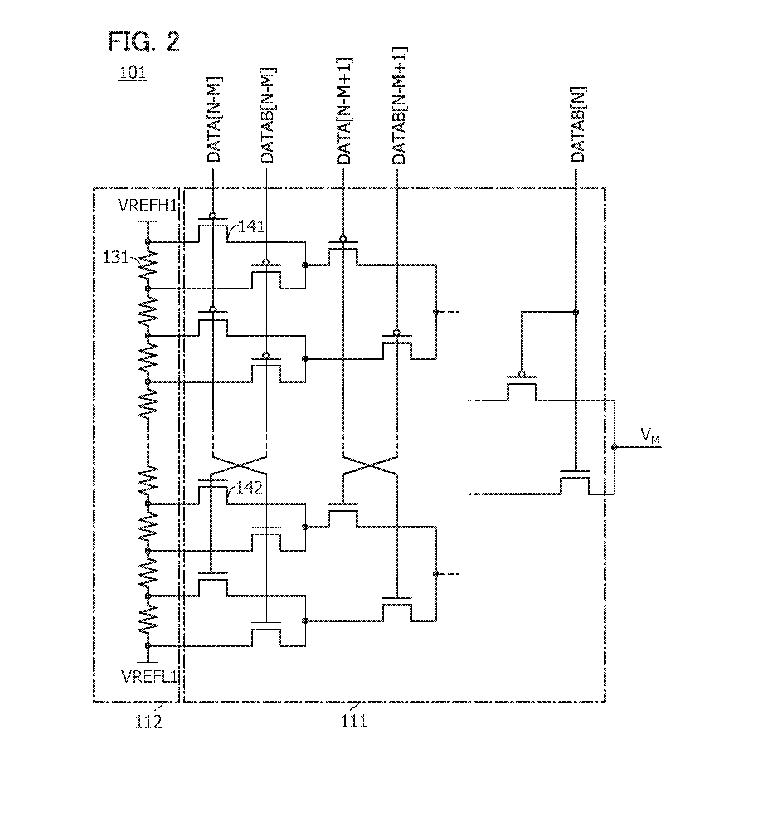
[0089]The source driver 200 can include the semiconductor device described in Embodiment 1. Specifically, the source driver 200 includes the decoder DEC and the semiconductor device 100. The semiconductor device 100 includes the voltage generator circuit 112, the voltage generator circuit 122, the pass transistor logic 111, the pass...

embodiment 3

[0104]In this embodiment, an example of a cross-sectional structure of a semiconductor device in one embodiment of the present invention will be described with reference FIG. 11.

[0105]In the semiconductor device shown in Embodiment 1, the D / A converter circuit 101, the D / A converter circuit 102, the voltage-current converter circuit 103, and the interpolation circuit 104 are formed using transistors containing silicon or the like. As silicon, polycrystalline silicon, microcrystalline silicon, or amorphous silicon can be used. Note that an oxide semiconductor or the like can be used instead of silicon.

[0106]FIG. 11 is a schematic cross-sectional view of a semiconductor device of one embodiment of the present invention. The semiconductor device in the schematic cross-sectional view of FIG. 11 includes an n-channel transistor and a p-channel transistor that contain a semiconductor material (e.g., silicon).

[0107]An n-channel transistor 510 includes a channel formation region 501 in a su...


PUM


Abstract

A semiconductor device with a novel structure. An upper-bit grayscale voltage and a lower-bit grayscale voltage are separately produced, and then the grayscale voltages are converted into currents and the currents are synthesized. The obtained current is converted into a voltage, and thus an intended grayscale voltage is obtained. The upper-bit grayscale voltage and the lower-bit grayscale voltage are generated using respective D/A converter circuits each including a resistor string circuit and a pass transistor logic. The increase in the number of transistors supplied with high voltage, which occurs along with the increase in the number of digital signal bits, is prevented. Thus, the increase in parasitic capacitance can be suppressed, and a smaller circuit area and higher response speed are obtained.

Description

BACKGROUND OF THE INVENTION[0001]1. Field of the Invention[0002]One embodiment of the present invention relates to a semiconductor device, an electronic component, and an electronic device.[0003]Note that one embodiment of the present invention is not limited to the above technical field. The technical field of the invention disclosed in this specification and the like relates to an object, a method, or a manufacturing method. In addition, one embodiment of the present invention relates to a process, a machine, manufacture, or a composition of matter. Specific examples of the technical field of one embodiment of the present invention disclosed in this specification include a semiconductor device, a display device, a light-emitting device, a power storage device, a memory device, a method for driving any of them, and a method for manufacturing any of them.[0004]In this specification and the like, a semiconductor device refers to an element, a circuit, a device, or the like that can f...

Claims


Application Information

Patent Timeline
Patent Type & Authority Applications(United States)
IPC IPC(8): H03M1/68G09G3/20H03K5/13
CPCH03M1/68H03K5/13G09G3/2003G09G2310/0291G09G2300/0828G09G2310/027H03K2005/00286G09G3/32G09G3/3688G09G3/3696H03M1/76
Inventor TAKAHASHI, KEI
Owner SEMICON ENERGY LAB CO LTD
Why Eureka
Try Eureka