Semiconductor device, display module, and electronic device

a technology of semiconductor devices and display modules, applied in the direction of static storage, digital storage, instruments, etc., can solve the problems of increasing the degree of wiring congestion in the driver's ic, and the display quality is reduced, and achieves the effect of increasing the degree of freedom of choi

Active Publication Date: 2020-08-04
SEMICON ENERGY LAB CO LTD
View PDF85 Cites 0 Cited by
  • Summary
  • Abstract
  • Description
  • Claims
  • Application Information

AI Technical Summary

Benefits of technology

[0008]As described above, there are a variety of structures of semiconductor devices functioning as driver ICs. The structures have merits and demerits, and an appropriate structure is selected depending on circumstances. Thus, a proposal for a semiconductor device that has a novel structure and functions as a driver IC leads to higher degree of freedom of choice.
[0012]In view of the above, an object of one embodiment of the present invention is to provide a novel semiconductor device or the like the frame of which can be narrower in spite of an increase in the number of output terminals. Another object of one embodiment of the present invention is to provide a novel semiconductor device or the like in which the degree of wiring congestion is decreased. Another object of one embodiment of the present invention is to provide a novel semiconductor device or the like with improved display quality.
[0021]According to one embodiment of the present invention, a novel semiconductor device or the like the frame of which can be narrower in spite of an increase in the number of output terminals can be provided. According to one embodiment of the present invention, a novel semiconductor device or the like in which the degree of wiring congestion is decreased can be provided. According to one embodiment of the present invention, a novel semiconductor device or the like with improved display quality can be provided.

Problems solved by technology

With an increase in the number of output terminals, the degree of wiring congestion in a driver IC is increased.
An increase in parasitic capacitance or parasitic resistance might cause a decrease in display quality.

Method used


Image

  • Semiconductor device, display module, and electronic device
  • Semiconductor device, display module, and electronic device
  • Semiconductor device, display module, and electronic device

Examples


embodiment 1

[0042]In this embodiment, an example of a semiconductor device functioning as a driver IC will be described.

[0043]In this specification and the like, a semiconductor device means any device that can function by utilizing semiconductor characteristics; thus, a driver IC composed of semiconductor elements such as transistors and a display device including the driver IC are included in the category of the semiconductor device.

[0044]A semiconductor device of one embodiment of the present invention is applied to a driver IC functioning as a source driver, in the following description. Therefore, a source driver and a driver IC are each also referred to as a semiconductor device.

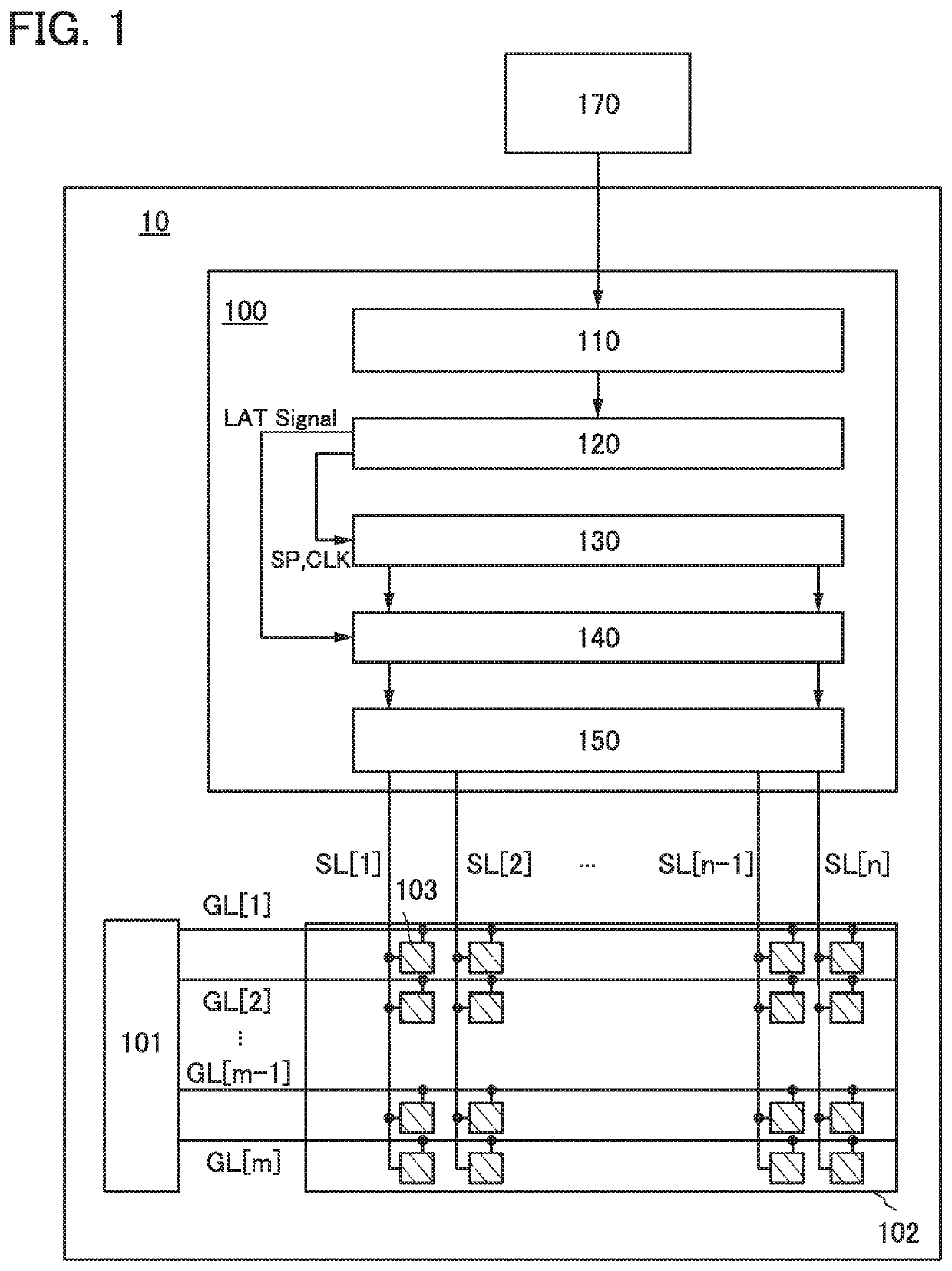
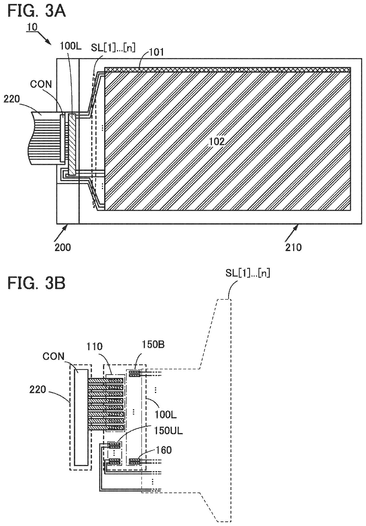
[0045]FIG. 1 is a block diagram of a display device 10 including a source driver. The display device 10 includes a source driver 100, a gate driver 101, and a display portion 102.

[0046]The display portion 102 includes pixels 103 arranged in a matrix. Each of the pixels 103 is connected to one of source lines SL[1]...

embodiment 2

[0094]In this embodiment, an example of a circuit configuration of the shift register described in the above embodiment and an example of a circuit configuration of a pixel in the display portion described in the above embodiment will be described.

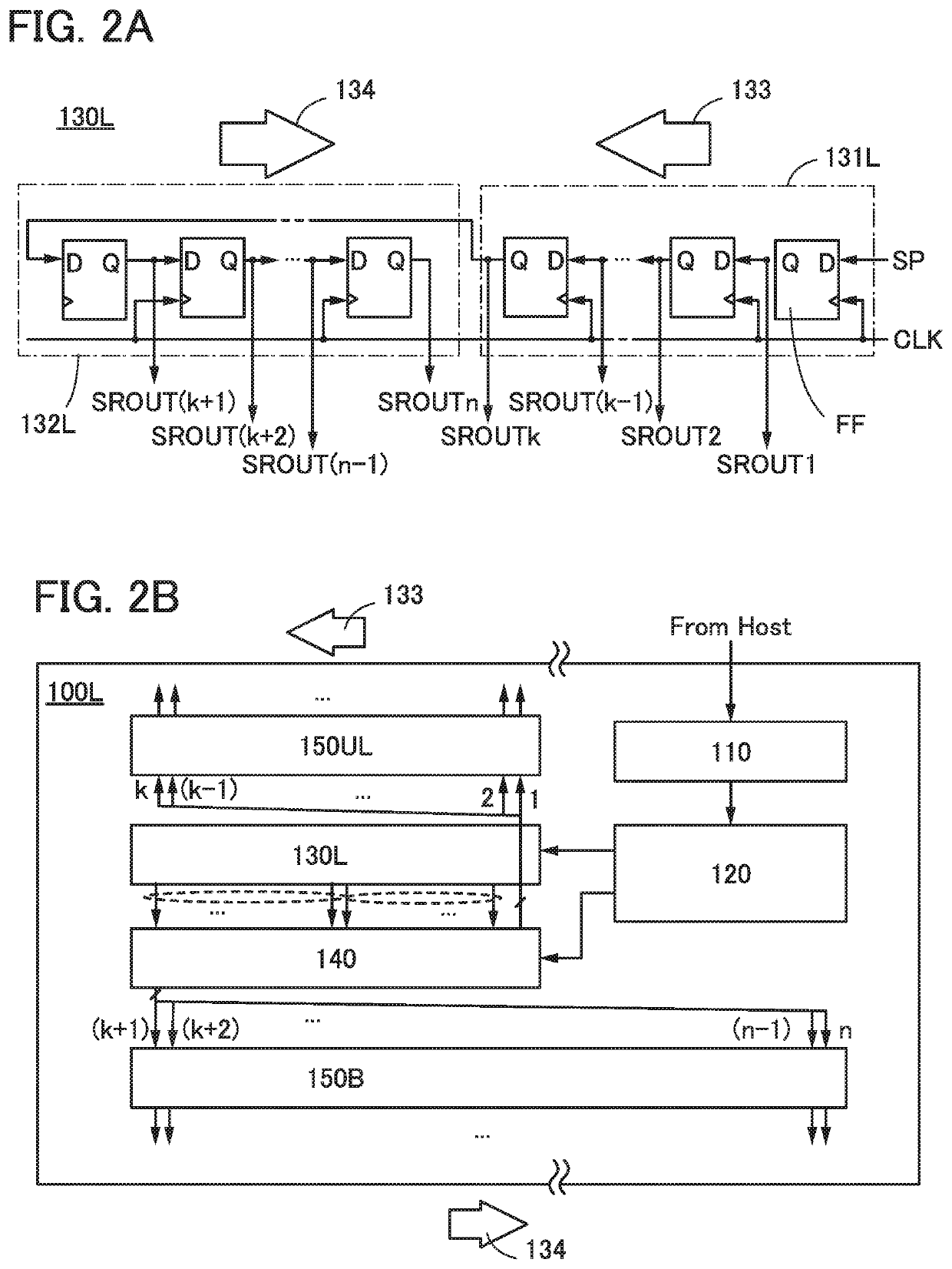
[0095]FIGS. 8A and 8B illustrate, as one example, a circuit configuration of a static shift register including a plurality of stages of pulse output circuits.

[0096]In the shift register illustrated in FIGS. 8A and 8B, a plurality of pulse output circuits FFs are connected in cascade. The plurality of stages of pulse output circuits FFs are connected to wirings through which a clock signal (CLK1) and a clock signal (CLK2) are transmitted. The pulse output circuit FF in the first stage is connected to a wiring through which a start pulse (SP) is transmitted. Output signals SROUT1 to SROUTn are output from the plurality of stages of pulse output circuits FFs.

[0097]The pulse output circuit FF includes, as illustrated in FIG. 8B, a switch 311, ...

embodiment 3

[0107]In this embodiment, an example of a cross-sectional structure of a semiconductor device in one embodiment of the present invention will be described with reference FIG. 10.

[0108]In the semiconductor device described in the above embodiment, the circuits such as the shift register circuit can be formed using a transistor including silicon. As silicon, polycrystalline silicon, microcrystalline silicon, or amorphous silicon can be used. Note that an oxide semiconductor or the like can be used instead of silicon.

[0109]FIG. 10 is a schematic cross-sectional view of a semiconductor device of one embodiment of the present invention. The semiconductor device in the schematic cross-sectional view of FIG. 10 includes an n-channel transistor and a p-channel transistor that contain a semiconductor material (e.g., silicon).

[0110]An n-channel transistor 510 includes a channel formation region 501 in a substrate 500 containing a semiconductor material, low-concentration impurity regions 502 ...


PUM


Abstract

A semiconductor device in which an increase in the degree of wiring congestion due to an increase in the number of output terminals of a driver IC can be reduced is provided. In a shift register of the driver IC, pulse signals are sequentially output in different directions. For example, pulse signal output circuits are provided so as to sequentially output pulse signals in ascending order from right to left and then sequentially output pulse signals in ascending order from left to right. With such a structure, output signals of the driver IC can be output not only from a side opposite to a side along which an input terminal is provided, but also from a side along which the input terminal is provided; thus, the number of output terminals can be increased without an increase in the degree of wiring congestion.

Description

BACKGROUND OF THE INVENTION[0001]1. Field of the Invention[0002]One embodiment of the present invention relates to a semiconductor device, a display module, and an electronic device.[0003]Note that one embodiment of the present invention is not limited to the above technical field. The technical field of the invention disclosed in this specification and the like relates to an object, a method, or a manufacturing method. In addition, one embodiment of the present invention relates to a process, a machine, manufacture, or a composition of matter. Specifically, examples of the technical field of one embodiment of the present invention disclosed in this specification include a semiconductor device, a display device, a light-emitting device, a power storage device, a memory device, a method for driving any of them, and a method for manufacturing any of them.[0004]In this specification and the like, a semiconductor device refers to an element, a circuit, a device, or the like that can fun...

Claims


Application Information

Patent Timeline
Patent Type & Authority Patents(United States)
IPC IPC(8): G11C19/28G09G3/3275G09G3/36
CPCG09G3/3275G11C19/28G09G3/3688G09G2300/0426G09G2320/0223G09G2310/0286
Inventor KOBAYASHI, HIDETOMOTAKAHASHI, KEI
Owner SEMICON ENERGY LAB CO LTD
Why Eureka
Try Eureka