
Fingerprint sensor and method thereof

a fingerprint sensor and fingerprint technology, applied in the field of fingerprint sensors and fingerprint sensing methods, can solve the problems of limited and restricted sensing of fingerprint sensors, and the sum of the thickness of layers that electric signals can transmit through remains limited

Active Publication Date: 2017-04-20
EGIS TECH
View PDF4 Cites 0 Cited by
  • Summary
  • Abstract
  • Description
  • Claims
  • Application Information

AI Technical Summary

Benefits of technology

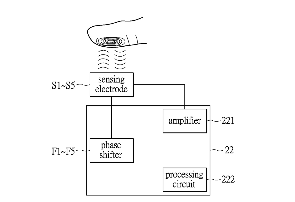
The present invention provides a fingerprint sensor and a related fingerprint sensing method that use a phase shifter to control the distribution of electric fields generated by sensing electrodes. This allows the electric signals to transmit through a thicker protection layer. The neighboring sensing electrodes are selectively turned on and groups of turned-on sensing electrodes are spaced by at least one turned-off sensing electrode to avoid direct coupling of electric fields and force the electric signals to transmit upward for a longer distance and through a thicker protection layer. The technical effect is improved accuracy and reliability in fingerprint sensing.

Problems solved by technology

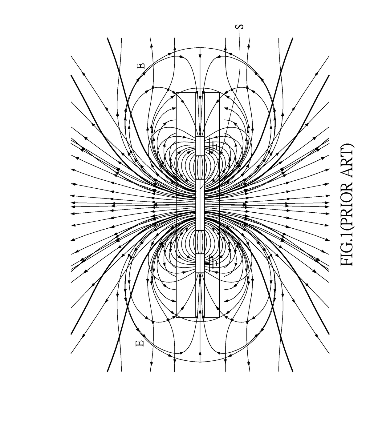
In terms of personal mobile devices using the fingerprint sensing technology, the sensibility of the fingerprint sensors is limited and restricted by the thickness of each structure layer which covers upon the sensing electrodes, such as the protection layer of the touch panel of the mobile device, because of the defocusing of the distribution of electric field.
However, as known by those skilled in the art, the sum of the thickness of layers that the electric signals can transmit through is still limited.

Method used


Image

  • Fingerprint sensor and method thereof
  • Fingerprint sensor and method thereof
  • Fingerprint sensor and method thereof

Examples


Embodiment Construction

[0018]The aforementioned illustrations and following detailed descriptions are exemplary for the purpose of further explaining the scope of the present invention. Other objectives and advantages related to the present invention will be illustrated in the subsequent descriptions and appended drawings.

[0019]It will be understood that, although the terms first, second, third, and the like, may be used herein to describe various elements, but these elements should not be limited by these terms. These terms are only to distinguish one element from another region or section discussed below and could be termed a second element without departing from the teachings of the instant disclosure. As used herein, the term “and / or” includes any and all combinations of one or more of the associated listed items.

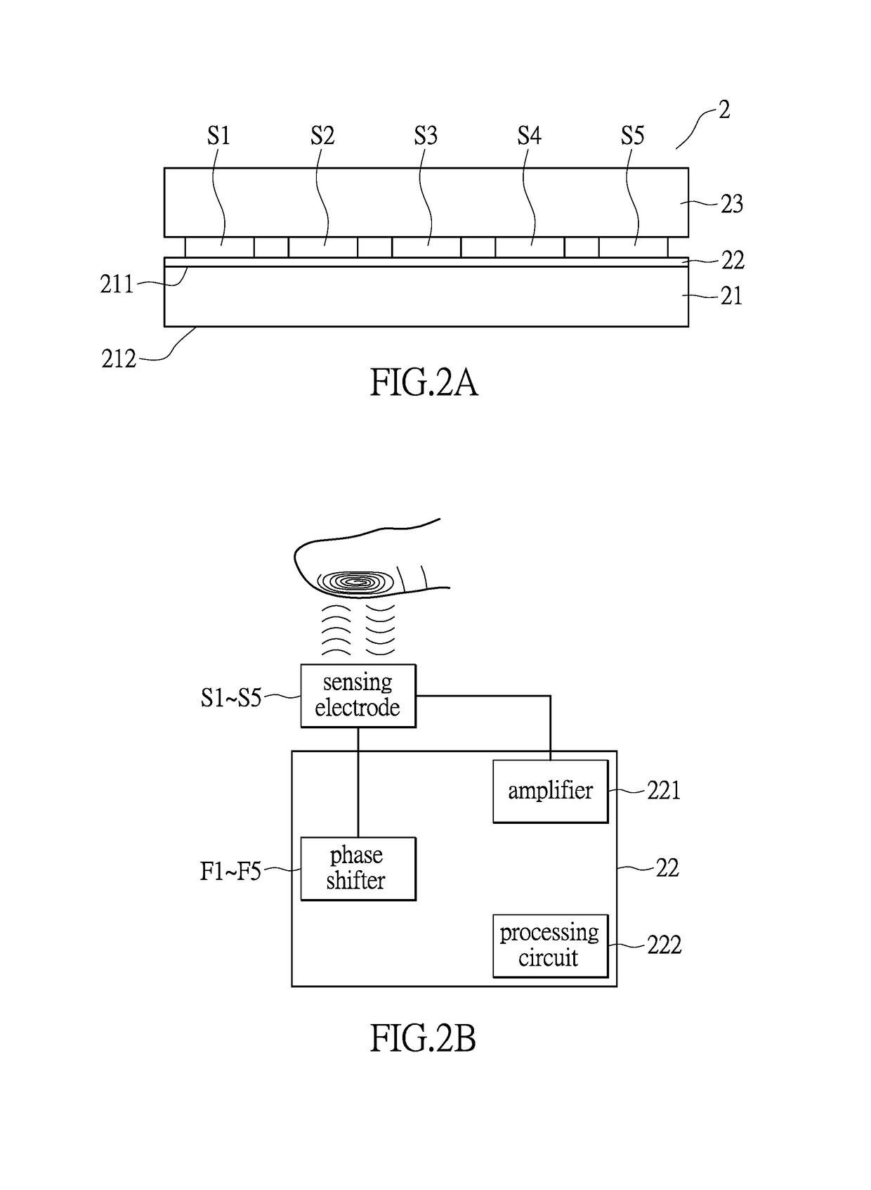
[0020]Please refer to FIG. 2A and FIG. 2B. FIG. 2A shows a schematic diagram of a fingerprint sensor of one embodiment of the present invention, and FIG. 2B shows a block diagram of a fingerp...


PUM


Abstract

Disclosed are a fingerprint sensor and a fingerprint sensing method thereof. The fingerprint sensor comprises a substrate, a plurality of sensing electrodes, an integrated circuit and a protection layer. The substrate has a first surface and a second surface. The sensing electrodes are configured on the first surface of the substrate, and electrically connected to the integrated circuit. The integrated circuit comprises a plurality of phase shifters, and each phase shifter is electrically connected to its corresponding sensing electrode to control the phase of electric signal transmitted by the sensing electrode. The first surface of the substrate is covered by the protection layer.

Description

BACKGROUND OF THE INVENTION[0001]1. Field of the Invention[0002]The present invention relates to a fingerprint sensor and a fingerprint sensing method; in particular, to a fingerprint sensor and a fingerprint sensing method that can improve the defocusing of electric field distribution.[0003]2. Description of Related Art[0004]In recent years, mobile devices have been widely used by people. Particularly, those personal mobile devices having touch panels have become an essential tool in our daily life and at work. To comply with safety requirements, those personal mobile devices are usually installed with a code locking process, and the codes could be numbers, patterns or biometric features, such as fingerprints.[0005]In terms of personal mobile devices using the fingerprint sensing technology, the sensibility of the fingerprint sensors is limited and restricted by the thickness of each structure layer which covers upon the sensing electrodes, such as the protection layer of the touch...

Claims


Application Information

Patent Timeline
Patent Type & Authority Applications(United States)
IPC IPC(8): G06K9/00
CPCG06K9/00087G06K9/00013G06V40/1318G06V40/1306G06F3/03547G06V40/1365G06V40/12
Inventor LIN, TODD
Owner EGIS TECH
Learn More