Array substrate, display panel, display device, and fabrication method thereof

a display device and substrate technology, applied in the field of array substrates, display panels, display devices, can solve the problems of inconvenient development of thinner and lighter display devices, large area occupied by wiring, and complicated wiring of touch-control structures in existing self-capacitive touch-control display devices

Active Publication Date: 2017-06-15
SHANGHAI AVIC OPTOELECTRONICS +1
View PDF9 Cites 8 Cited by
  • Summary
  • Abstract
  • Description
  • Claims
  • Application Information

AI Technical Summary

Benefits of technology

[0005]One aspect of the present disclosure includes an array substrate. The array substrate includes a plurality of pixel units defined by intersected gate electrode lines and data lines, a plurality of independent touch-control electrodes arranged in an array, and a touch-control circuit. The touch-control circuit includes a plurality of first switch units, a plurality of first control leads, a plurality of touch-detection terminals, and a control unit. The touch-control electrode is electrically connected to one touch-control terminal through at least one of the first switch units. The first switch unit is electrically connected to the control unit through at least one of the first control leads. The first control lead is configured between any of neighboring rows of the pixel units. Further, when the array substrate is in a touch detection phase, the control unit is capable of controlling an ON status of the first switch units to allow row-by-row control of touch detection for the plurality of touch-control electrodes.

Problems solved by technology

However, the wiring of touch-control structures in existing self-capacitive touch-control display devices may be quite complicated and the area occupied by the wiring may also be relatively large.
Therefore, the existing self-capacitive touch-control display devices may not be conducive to the development of thinner and lighter display devices.

Method used


Image

  • Array substrate, display panel, display device, and fabrication method thereof
  • Array substrate, display panel, display device, and fabrication method thereof
  • Array substrate, display panel, display device, and fabrication method thereof

Examples


Embodiment Construction

[0020]Reference will now be made in detail to exemplary embodiments of the invention, which are illustrated in the accompanying drawings. Wherever possible, the same reference numbers will be used throughout the drawings to refer to the same or like parts.

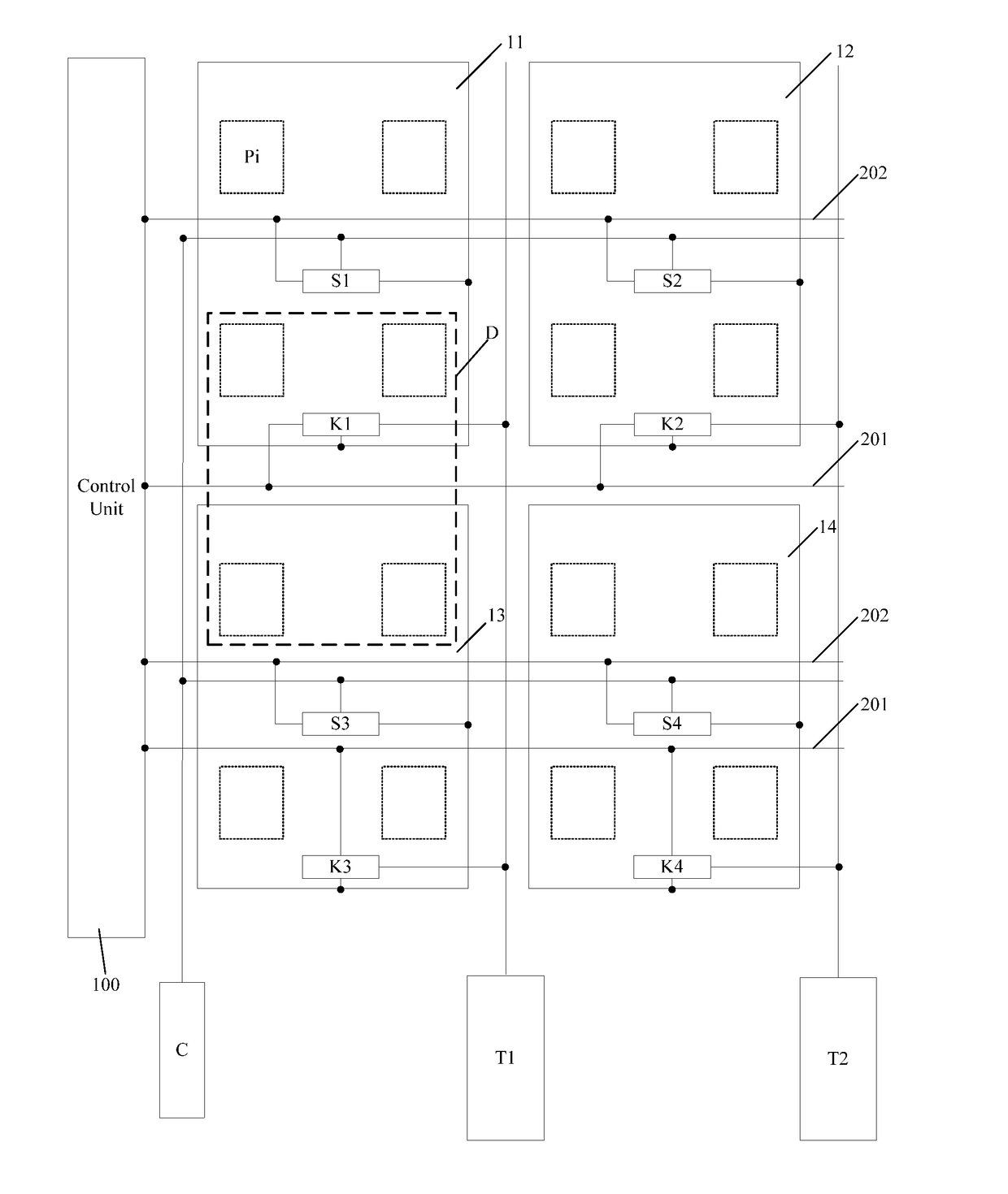
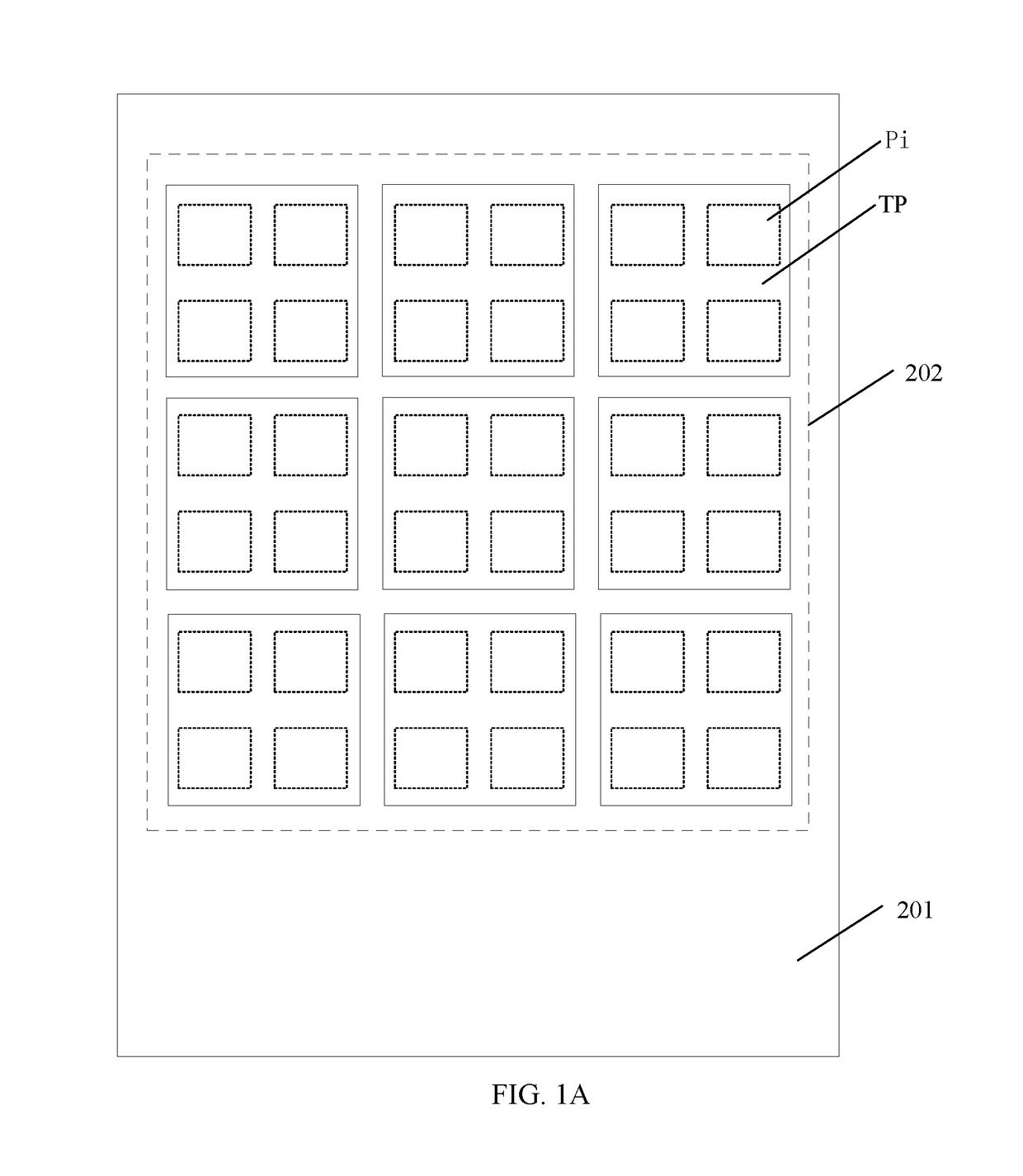
[0021]The present disclosure provides an array substrate. FIG. 1A shows a schematic view of an exemplary array substrate consistent with disclosed embodiments.

[0022]Referring FIG. 1A, an array substrate includes a non-display region 201 and a display region 202. The display region 202 includes a plurality of pixel unites Pi and a plurality of touch-control electrodes TP. The plurality of pixels Pi is arranged in an array defined by a plurality of gate electrode lines and a plurality of data lines with the plurality of gate electrode lines intercepting with the plurality of data lines. Further, each pixel unit Pi includes a sub-pixel. The plurality of touch-control electrodes TP is also arranged into an array. The touch-control elec...


PUM


Abstract

An array substrate includes a plurality of pixel units defined by intersected gate electrode lines and data lines, a plurality of independent touch-control electrodes arranged in an array, and a touch-control circuit. The touch-control circuit includes a plurality of first switch units, a plurality of first control leads, a plurality of touch-detection terminals, and a control unit. The touch-control electrode is electrically connected to one touch-control terminal through at least one of the first switch units. The first switch unit is electrically connected to the control unit through at least one of the first control leads. The first control lead is configured between any of neighboring rows of the pixel units. Further, when the array substrate is in a touch detection phase, the control unit is capable of controlling an ON status of the first switch units to allow row-by-row control of touch detection for the plurality of touch-control electrodes.

Description

CROSS-REFERENCES TO RELATED APPLICATIONS[0001]This application claims the priority of Chinese patent application No. 201510926109.2, filed on Dec. 11, 2015, the entirety of which is incorporated herein by reference.BACKGROUND[0002]Touch-control display device is a device that allows user to enter user command by selecting displayed content either directly using hand or with assistance of other objects. When user uses hand or other objects to touch the screen of a touch-control display device, the touch-control display device detects the touch point and then converts the touch point to a corresponding command. Then, based on the entered command, the touch-control display device may be driven to realize a specific display.[0003]According to the operation principles, the existing touch-control display devices may fall into two categories: capacitive touch-control display device and inductive touch-control display device, respectively. The capacitive touch-control display device further...

Claims


Application Information

Patent Timeline
Patent Type & Authority Applications(United States)
IPC IPC(8): G06F3/041
CPCG06F3/0416G06F2203/04103G06F3/0412G06F3/044G06F3/04166
Inventor XI, KERUICUI, TINGTING
Owner SHANGHAI AVIC OPTOELECTRONICS
Why Eureka
Try Eureka