Information Processing Device, Display Device, and Electronic Device

a technology which is applied in the field of information processing device and display device, and an electronic device, can solve the problems of reducing portability, browsability of display and portability is difficult to improve, and achieves high portability and reliability, and high operability

Active Publication Date: 2017-11-02
SEMICON ENERGY LAB CO LTD
View PDF6 Cites 22 Cited by
  • Summary
  • Abstract
  • Description
  • Claims
  • Application Information

AI Technical Summary

Benefits of technology

[0017]According to one embodiment of the present invention, a novel information processing device with high portability and reliability can be provided. A novel information processing device with high operability can be provided. A novel information processing device, a novel display device, or the like can be provided. Not

Problems solved by technology

However, in portable electronic devices, an enlargement of display regions causes a reduction in portabi

Method used


Image

  • Information Processing Device, Display Device, and Electronic Device
  • Information Processing Device, Display Device, and Electronic Device
  • Information Processing Device, Display Device, and Electronic Device

Examples


embodiment 1

[0031]In this embodiment, a foldable touch panel that is included in an information processing device of one embodiment of the present invention will be described with reference to FIG. 1A to FIG. 4. The touch panel includes a display region and a touch sensor.

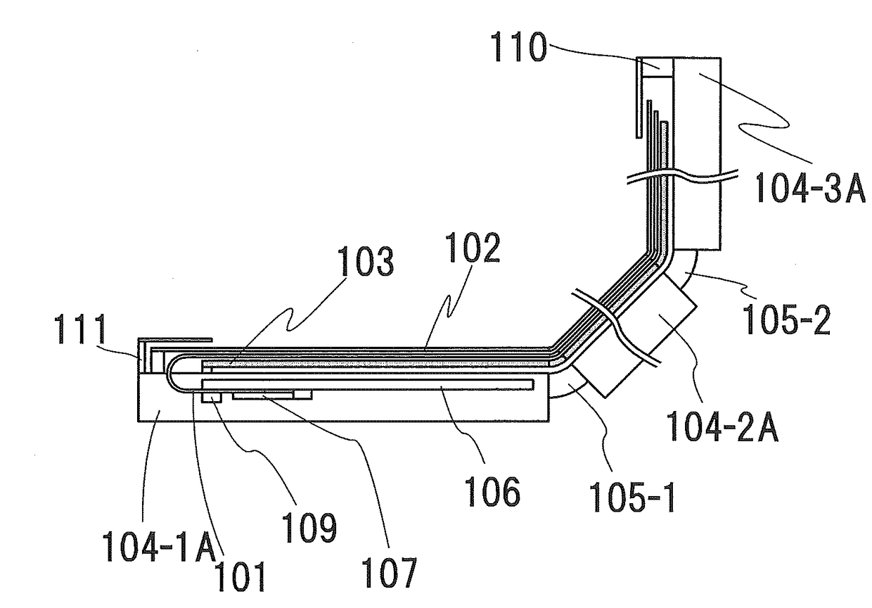
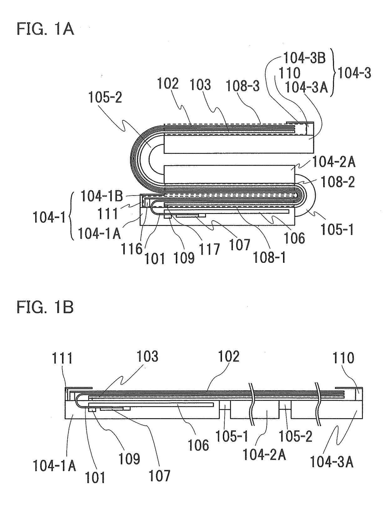
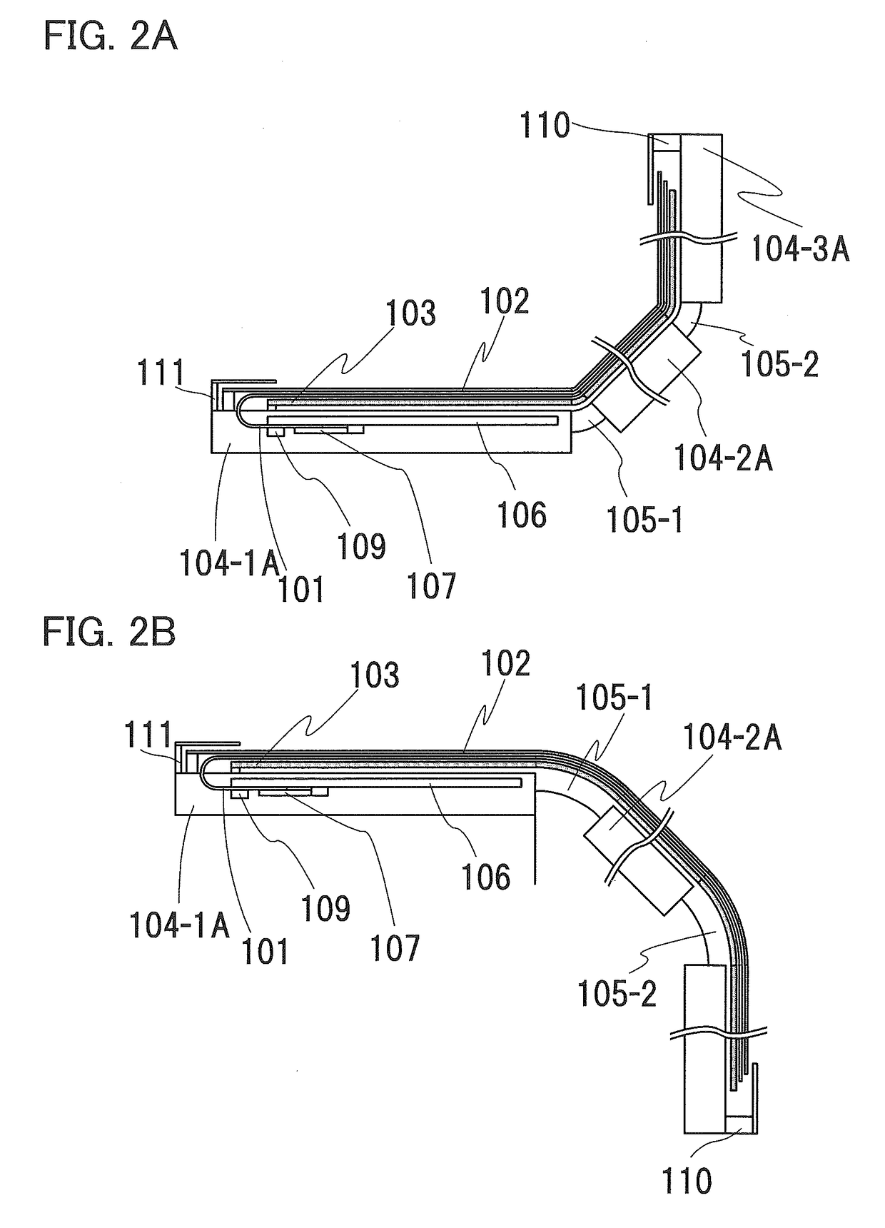
[0032]FIG. 1A is a cross-sectional view showing one state of a foldable information processing device of one embodiment of the present invention. FIG. 1B shows another state of the foldable information processing device of one embodiment of the present invention.

[0033]In one embodiment of the present invention, the foldable information processing device includes a panel substrate 101, a first film 102, a second film 103, a first housing 104-1, a second housing 104-2 (see FIG. 4), a third housing 104-3, a hinge 105-1, a hinge 105-2, a circuit board 106, and an FPC 107. The panel substrate 101, the first film 102, and the second film 103 each have flexibility. The first housing 104-1, the second housing 104-2, or the third housi...

embodiment 2

[0064]In this embodiment, a foldable touch panel that is included in an information processing device of one embodiment of the present invention will be described with reference to FIGS. 5A to 5C.

[0065]FIG. 5A is a top view illustrating a structure of the touch panel that can be used in the information processing device of one embodiment of the present invention. The components in FIG. 5A correspond to those in FIG. 3A.

[0066]FIG. 5B is a cross-sectional view along line A-B and line C-D in FIG. 5A.

[0067]FIG. 5C is a cross-sectional view along line E-F in FIG. 5A.

[0068]The touch panel 300 includes a substrate 310 and a counter substrate 370 that faces the substrate 310 (see FIG. 5B).

[0069]When a material having flexibility is used for the substrate 310 and the counter substrate 370, the touch panel 300 can have flexibility.

[0070]Note that when the flexible touch panel 300 is changed in its form, stress is applied to a functional element provided in the touch panel 300. Preferably, the...

embodiment 3

[0097]In this embodiment, a structure of a flexible touch panel that can be used in the panel substrate of the information processing device of one embodiment of the present invention will be described with reference to FIGS. 6A and 6B and FIGS. 7A to 7C.

[0098]FIG. 6A is a perspective view of a touch panel 500 exemplified in this embodiment. Note that FIGS. 6A and 6B illustrate only main components for simplicity. FIG. 6B is a perspective view of the touch panel 500.

[0099]FIG. 7A is a cross-sectional view of the touch panel 500 along X1-X2 in FIG. 6A.

[0100]The touch panel 500 includes a display portion 501 and a touch sensor 595 (see FIG. 6B). Furthermore, the touch panel 500 includes a substrate 510, a substrate 570, and a substrate 590. Note that the substrates 510, 570, and 590 each have flexibility.

[0101]The display portion 501 includes the substrate 510, a plurality of pixels over the substrate 510, a plurality of wirings 511 through which signals are supplied to the pixels, an...


PUM


Abstract

An electronic device with a large display region and improved portability is provided. An electronic device with improved reliability is provided. The information processing device includes a first film, a second film, a panel substrate, and at least a first housing. The panel substrate has flexibility and includes a display region. The first film has visible light transmittance and flexibility, and the second film has flexibility. The first housing includes a first slit, the panel substrate includes a region interposed between the first film and the second film, the first slit is configured to store the region, and one or more of the panel substrate, the first film, and the second film can slide along the first slit.

Description

BACKGROUND OF THE INVENTION1. Field of the Invention[0001]One embodiment of the present invention relates to an information processing device, a display device, and an electronic device.[0002]Note that one embodiment of the present invention is not limited to the above technical field. The technical field of one embodiment of the invention disclosed in this specification and the like relates to an object, a method, or a manufacturing method. Furthermore, one embodiment of the present invention relates to a process, a machine, manufacture, or a composition of matter. Specifically, examples of the technical field of one embodiment of the present invention disclosed in this specification include a semiconductor device, a display device, a light-emitting device, a power storage device, a memory device, a method for driving any of them, and a method for manufacturing any of them.2. Description of the Related Art[0003]Electronic devices including display devices have recently been diversi...

Claims


Application Information

Patent Timeline
IPC IPC(8): G06F1/16G06F3/041G06F3/044
CPCG06F1/1652G06F2203/04102G06F3/0416G06F3/044G06F3/0412G06F3/042G06F2203/04103G06F2203/04111G06F1/1616G06F1/1618G06F1/1641G06F1/1675G06F3/0446G06F3/0443H10K59/40
Inventor ISA, TOSHIYUKIENDO, AKIOTSUKAMOTO, YOSUKEKOYAMA, JUN
Owner SEMICON ENERGY LAB CO LTD
Why Eureka
Try Eureka