Supercharge Your Innovation With Domain-Expert AI Agents!

Fingerprint sensors with ESD protection

a fingerprint sensor and protection technology, applied in the field of fingerprint sensors, can solve the problems of esd protection options often running into a fundamental limitation, fingerprint sensors are prone to various levels of esd voltage, and image quality may be deteriorated

Active Publication Date: 2018-04-19
NEXT BIOMETRICS GRP
View PDF0 Cites 8 Cited by
  • Summary
  • Abstract
  • Description
  • Claims
  • Application Information

AI Technical Summary

Problems solved by technology

This close proximity means that the fingerprint sensor is prone to various levels of ESD voltage and the ESD will have a high concentration over a smaller area.
This environment presents a unique challenge for optimizing among ESD protection, mechanical stress tolerance, and thermal signal sensitivity.
However, these ESD mitigation options often run into a fundamental limitation of the capacitive fingerprint sensor: tradeoff between ESD protection effectiveness and sensing resolution.
Due to the operating mechanism of a capacitive fingerprint sensor, there has to be a certain distance between the ESD units and the active electrode when in the same plane, and they cannot be overlapped if in different planes, otherwise image quality may be deteriorated and resolution may be reduced.
Thus, the amount of these ESD units are typically limited to less than 10% of the active electrode, which limits the ESD protection effectiveness.
However this scheme is only effective if the finger touches the peripheral area.
That is, it offers no ESD protection over the active area which is the primary concern.

Method used


Image

  • Fingerprint sensors with ESD protection
  • Fingerprint sensors with ESD protection
  • Fingerprint sensors with ESD protection

Examples


production examples

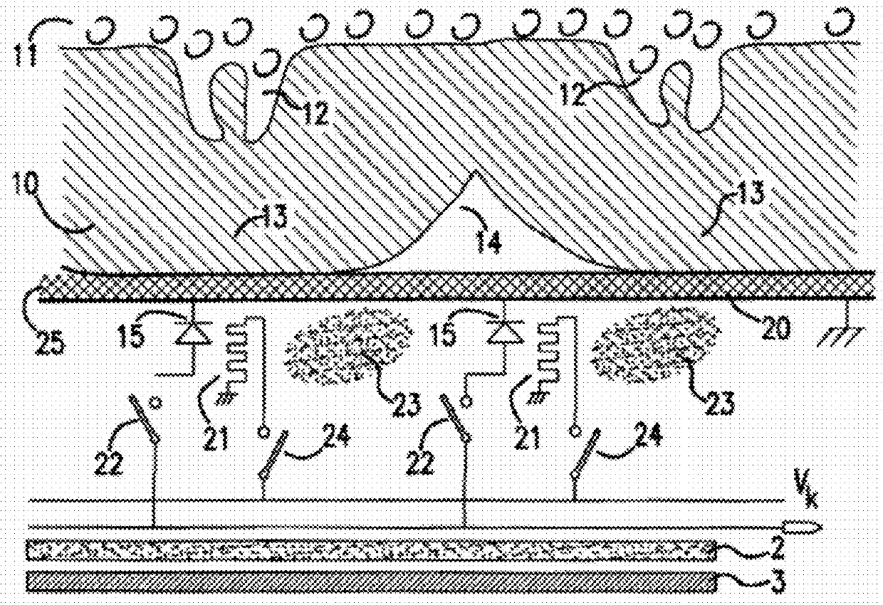
[0064]As described below, fingerprint sensors were fabricated with disclosed ESD protection approaches. ESD performance, scratch resistance, and reliability were tested.

1st Production Example

[0065]The first production example of the fingerprint sensor was implemented with the structure described in connection with FIG. 9, where an ESD protection layer 80 is disposed over the entire second insulating layer 66 like a blanket, followed by application of the hard coat layer 68. The ESD protection layer 80 was disposed onto a contact pad connected to external ground. The second insulating layer 66 was a 5000 Å-thick silicon nitride layer deposited though plasma-enhanced chemical vapor deposition (PECVD). The ESD protection layer 80 was a 2000 Å thick Molybdenum (Mo) layer, with a sheet resistance of approximately 0.6 ohm / sq. The hard coat layer was a 1900 Å-thick silicon nitride layer followed by a PECVD deposited 1.2 μm-thick Diamond-Like-Carbon (DLC) layer.

[0066]ESD performance was tes...


PUM


Abstract

A fingerprint sensing device includes a substrate; a plurality of pixels arranged in a grid of rows and columns, each pixel having an active thermal sensing element therein; a first metal layer forming first addressing lines for addressing the active thermal sensing elements; a second metal layer above the first metal layer and forming second addressing lines for addressing the active thermal sensing elements; an electrically conductive ESD protection layer; and an insulating layer disposed between the ESD protection layer and the active thermal sensing elements. The ESD protection layer is electrically connected to a bias potential. The ESD protection layer is disposed in a pattern such that it partially overlaps each pixel, the ESD protection layer at least partially overlapping the active thermal sensing element of each pixel.

Description

CROSS REFERENCE TO RELATED APPLICATIONS[0001]This application claims priority to U.S. Provisional Patent Application Ser. No. 62 / 408,177 filed Oct. 14, 2016, the entirety of which is incorporated herein by reference.TECHNICAL FIELD[0002]The present invention relates to fingerprint sensors, and more particularly to electrostatic discharge (ESD) protection for fingerprint sensors.BACKGROUND[0003]Fingerprint sensors employing the so-called “active thermal principle” are disclosed in U.S. Pat. Nos. 6,091,837 and 7,910,902, both to Ngoc Minh Dinh. The basic principle of the active thermal fingerprint sensor is the use of an array of PIN diodes as thermal sensors to differentiate the ridges and valleys of the human fingerprint since the heat transfer in these two areas are different. (A PIN diode is a diode with a wide, undoped intrinsic semiconductor region between a p-type semiconductor and an n-type semiconductor region. The p-type and n-type regions are typically heavily doped to form...

Claims


Application Information

Patent Timeline
Patent Type & Authority Applications(United States)
IPC IPC(8): G06K9/00H01L27/02
CPCG06K9/00053G06K9/0002G06K9/00087H01L27/0255G06V40/1329G06V40/1306G06V40/1365
Inventor TROCCOLI, MATIAS N.PANG, HUIQINGKWAN, KING HONGSHAFFER, JAMIE LYN
Owner NEXT BIOMETRICS GRP
Features
  • R&D
  • Intellectual Property
  • Life Sciences
  • Materials
  • Tech Scout
  • Unparalleled Data Quality
  • Higher Quality Content
  • 60% Fewer Hallucinations
Learn More