Fabrication of fin field effect transistors utilizing different fin channel materials while maintaining consistent fin widths

a technology of fin field and transistor, which is applied in the direction of transistors, semiconductor devices, electrical equipment, etc., can solve the problems of difficult electrical contacts and difficult formation of individual components

Active Publication Date: 2018-08-30
IBM CORP
View PDF9 Cites 28 Cited by
  • Summary
  • Abstract
  • Description
  • Claims
  • Application Information

AI Technical Summary

Benefits of technology

[0007]In accordance with yet another embodiment of the present invention, a semiconductor device with vertical fins made of different materials, including, one or more vertical fins formed on a first region of a substrate, wherein each of the one or more vertical fins formed on a first region of a substrate includes a fin core made of a same material as the substrate, and one or more vertical fin

Problems solved by technology

With ever decreasing device dimensions, forming the individu

Method used


Image

  • Fabrication of fin field effect transistors utilizing different fin channel materials while maintaining consistent fin widths
  • Fabrication of fin field effect transistors utilizing different fin channel materials while maintaining consistent fin widths
  • Fabrication of fin field effect transistors utilizing different fin channel materials while maintaining consistent fin widths

Examples


Embodiment Construction

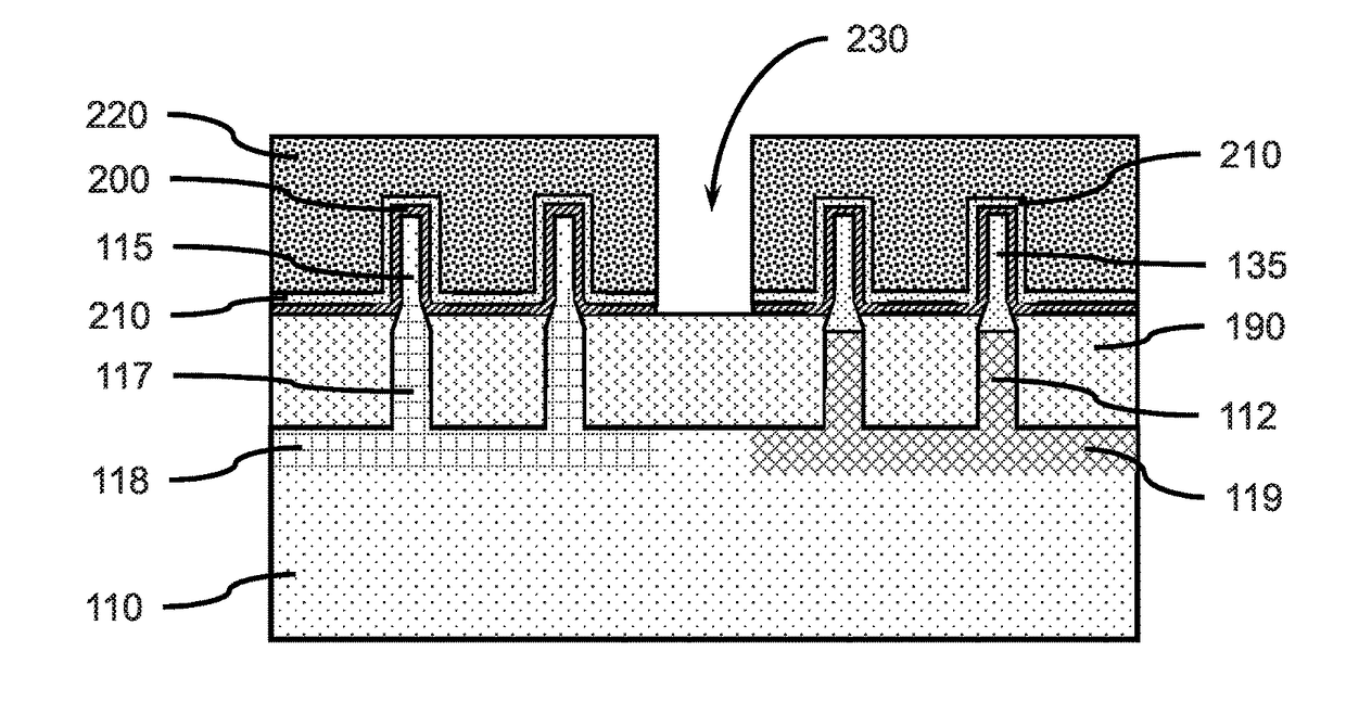
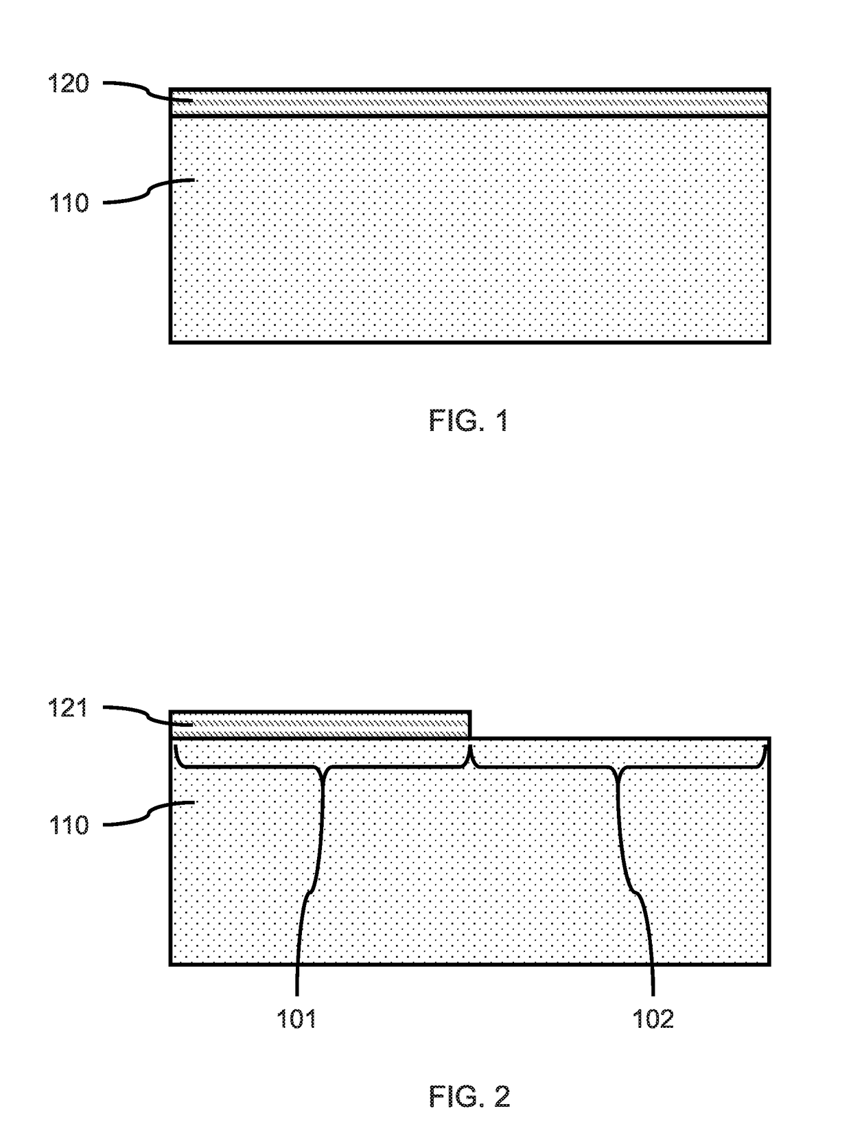
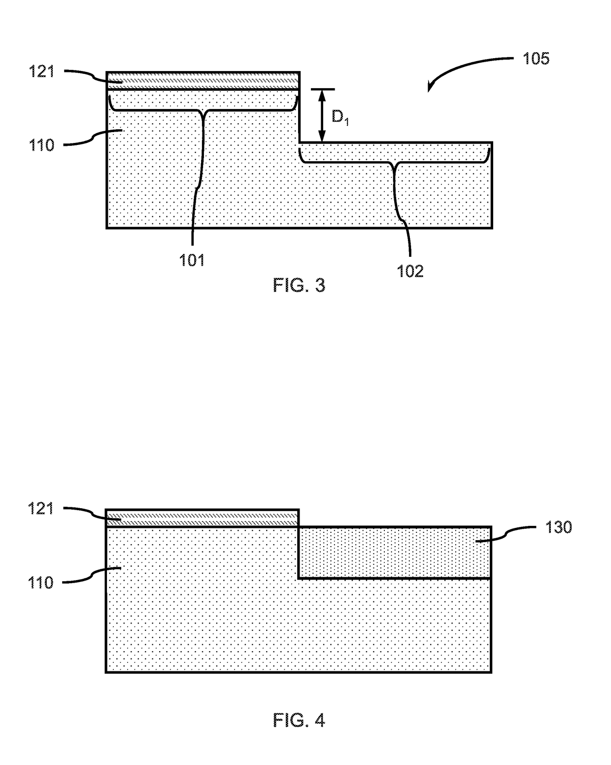
[0031]Principles and embodiments of the present invention relate generally to forming a set of vertical fins on a substrate, where the vertical fins of a first subset include a first material, and the vertical fins of a second subset include a second material different from the first material, such that the vertical fins may experience different responses to processing conditions. Different channel materials are desired for nFETs and pFETs so that the performances of the nFETs and pFETs can be altered and improved independently. With ever decreasing device dimensions, forming transistors from different materials becomes even more difficult. The formation of fin field effect transistors (FinFETs) with critical dimensions (i.e., line width, fin width) at or below 10 nanometers (nm) can involve utilizing different materials to accomplish the fabrication of device features in that size range. A specific challenge, however, is forming an nFET and a pFET from different materials with subs...


PUM


Abstract

A method of forming vertical fins on a substrate at the same time, the method including, forming a mask segment on a first region of the substrate while exposing the surface of a second region of the substrate, removing a portion of the substrate in the second region to form a recess, forming a fin layer in the recess, where the fin layer has a different material composition than the substrate, and forming at least one vertical fin on the first region of the substrate and at least one vertical fin on the second region of the substrate, where the vertical fin on the second region of the substrate includes a fin layer pillar formed from the fin layer and a substrate pillar.

Description

BACKGROUNDTechnical Field[0001]The present invention generally relates to formation of multiple vertical fins, where neighboring fins have different material compositions, and more particularly to fabricating fin field effect transistors (FinFETs) having fin channels with different material compositions, while avoiding disparities in channel width due to material related processing characteristics.Description of the Related Art[0002]A Field Effect Transistor (FET) typically has a source, a channel, and a drain, where current flows from the source to the drain, and a gate that controls the flow of current through the channel. Field Effect Transistors (FETs) can have a variety of different structures, for example, FETs have been fabricated with the source, channel, and drain formed in the substrate material itself, where the current flows horizontally (i.e., in the plane of the substrate), and finFETs have been formed with the channel extending outward from the substrate, but where th...

Claims


Application Information

Patent Timeline
IPC IPC(8): H01L27/092H01L29/66H01L21/02H01L29/10H01L27/088H01L21/8238H01L21/8234H01L29/161
CPCH01L27/0924H01L29/66795H01L21/02532H01L29/1083H01L29/161H01L27/0886H01L21/823821H01L21/823431H01L21/02381H01L21/823807H01L29/1054H01L29/66818
Inventor CHENG, KANGGUOLI, JUNTAOXU, PENG
Owner IBM CORP
Why Eureka
Try Eureka