Array substrate of OLED display device and method for manufacturing the same

a technology of array substrate and display device, which is applied in the field of array substrate of oled display device, can solve the problems that the requirements for different electrical properties of the first thin-film transistor and the second thin-film transistor cannot be m

Active Publication Date: 2018-11-22
TCL CHINA STAR OPTOELECTRONICS TECH CO LTD
View PDF5 Cites 0 Cited by
  • Summary
  • Abstract
  • Description
  • Claims
  • Application Information

AI Technical Summary

Benefits of technology

[0007]The present disclosure aims to provide an array substrate of an OLED display device and a method for manufacturing the same, so that thin-film transistors having different functions can have different electrical properties.
[0026]The present disclosure has following beneficial effects. In the array substrate of the OLED display device provided herein, both the first thin-film transistor and the second thin-film transistor have a top gate structure. The gate of the first thin-film transistor is arranged on the first metal layer. A distance between the gate of the first thin-film transistor and the active channel layer thereof is equal to a thickness of the first insulating layer. Therefore, a sub-threshold of the first thin-film transistor is relatively small, and the first thin-film transistor can be turned on or turned off quickly. The gate of the second thin-film transistor is arranged on the second metal layer. A distance between the gate of the second thin-film transistor and the active channel layer thereof is equal to a sum of the thickness of the first insulating layer and a thickness of the second insulating layer. Thus, a sub-threshold of the second thin-film transistor is relatively large, which is beneficial for a grayscale debugging thereof. Therefore, the array substrate of the OLED display device provided in the present disclosure enables the first thin-film transistor and the second thin-film transistor to have different electrical properties, thereby improving display qualities of the OLED display device.

Problems solved by technology

Therefore, the requirements for different electrical properties of the first thin-film transistor and the second thin-film transistor cannot be met.

Method used


Image

  • Array substrate of OLED display device and method for manufacturing the same
  • Array substrate of OLED display device and method for manufacturing the same
  • Array substrate of OLED display device and method for manufacturing the same

Examples


Embodiment Construction

[0032]The implementation manner of the present disclosure will be explained in detail below with reference to the accompanying drawings and the embodiments, so that one can fully understand how the present disclosure solves the technical problem and achieves the technical effects through the technical means, thereby implementing the same. It should be noted that, as long as there is no conflict, any of the embodiments and any of the technical features thereof can be combined with one another, and the technical solutions obtained therefrom all fall within the scope of the present disclosure.

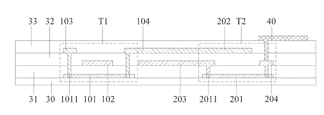
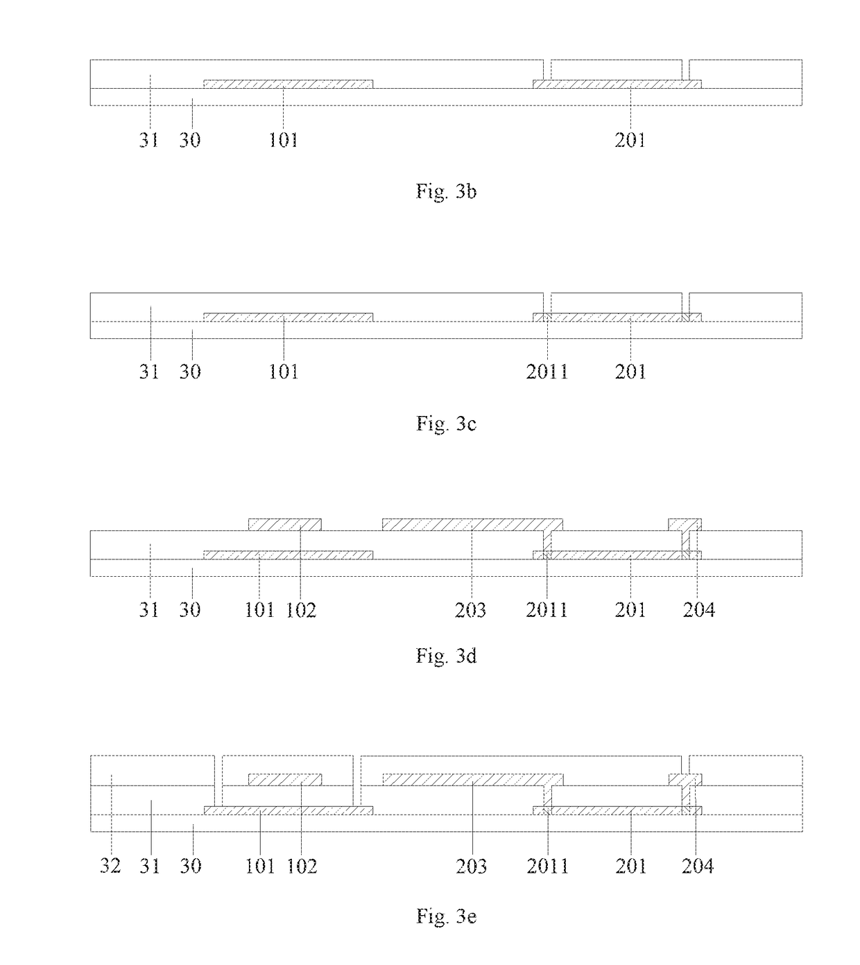
[0033]The present embodiment provides an array substrate of an OLED display device and a method for manufacturing the same, which enables thin-film transistors having different functions to have different electrical properties so as to improve display qualities of the OLED display device.

[0034]The array substrate of the OLED display device provided in the embodiment of the present disclosure compr...


PUM


Abstract

Disclosed are an array substrate of an OLED display device and a method for manufacturing the same. Thin-film transistors having different functions can have different electrical properties. The array substrate includes a base substrate, a semiconductor layer, a first insulating layer, a first metal layer, a second insulating layer, a second metal layer, and a third insulating layer which are arranged sequentially from bottom to top. A plurality of driving units are formed on the array substrate, and each of the driving units comprises a first thin-film transistor and a second thin-film transistor.

Description

CROSS-REFERENCE TO RELATED APPLICATIONS[0001]This application claims the priority of Chinese patent application CN201610630351.X, entitled “Array substrate of OLED display device and method for manufacturing the same” and filed on Aug. 3, 2016, the entirety of which is incorporated herein by reference.FIELD OF THE INVENTION[0002]The present disclosure relates to the technical field of display, and in particular, to an array substrate of an OLED display device and a method for manufacturing the same.BACKGROUND OF THE INVENTION[0003]With the development of display technologies, organic light-emitting diode (OLED) display technology gradually becomes mature and OLED display devices are increasingly used in different display fields.[0004]A basic driving unit in an OLED display device is shown in FIG. 1. The driving unit comprises two thin-film transistors (TFT) and a storage capacitor Cst to form a 2T1C structure. A scanning signal Vgate is input to a gate of a first thin-film transisto...

Claims


Application Information

Patent Timeline
Patent Type & Authority Applications(United States)
IPC IPC(8): H01L51/00H01L33/00
CPCH01L33/00H01L51/00H01L27/124H01L27/1259H10K59/131H10K59/1201H01L27/1225H01L27/1288H10K59/123H10K59/124H10K59/1213H10K99/00
Inventor SHI, LONGQIANG
Owner TCL CHINA STAR OPTOELECTRONICS TECH CO LTD
Why Eureka
Try Eureka