TFT backplate structure and manufacture method thereof

a technology of thin film transistors and backplates, applied in the field of display technology, can solve the problems of reducing the stability of these two structures, promoting yield and manufacturing cost, and achieving the effect of raising the performance of tft backplates

Active Publication Date: 2018-08-07
TCL CHINA STAR OPTOELECTRONICS TECH CO LTD
View PDF3 Cites 0 Cited by
  • Summary
  • Abstract
  • Description
  • Claims
  • Application Information

AI Technical Summary

Benefits of technology

[0009]An objective of the present invention is to provide a thin film transistor (TFT) backplate structure, capable of differentiating the switch TFT and the drive TFT to make the switch TFT and the drive TFT have different electrical properties and raise the performance of the TFT backplate.
[0010]Another objective of the present invention is to provide a manufacture method of a TFT backplate structure, capable of manufacturing the switch TFT and the drive TFT have different electrical properties thereby to raise the performance of the TFT backplate.
[0031]The benefits of the present invention are: according to the TFT backplate structure of the present invention, by arranging the first and second gate isolation layers having different materials or different thicknesses for differentiating the switch TFT and the drive TFT to make that the switch TFT possesses a smaller subthreshold swing for fast charge and discharge, and the drive TFT possesses a larger subthreshold swing for more precisely controlling the current and the grey scale. Accordingly, the switch TFT and the drive TFT have different electrical properties to raise the performance of the TFT backplate. According to the manufacture method of the TFT backplate structure, the first and second gate isolation layers are manufactured with different materials or different thicknesses so that the switch TFT and the drive TFT have different electrical properties to raise the performance of the TFT backplate.

Problems solved by technology

The stability is better but the manufacture of the etching stopper layer needs one extra mask and the coupling capacitance is larger which goes against the promotion of yield and decrease of manufacture cost.
However, the stabilities of these two structures have yet to be promoted.

Method used


Image

  • TFT backplate structure and manufacture method thereof
  • TFT backplate structure and manufacture method thereof
  • TFT backplate structure and manufacture method thereof

Examples


Embodiment Construction

[0048]In order to better understand the characteristics and technical aspect of the invention, reference is made to the following detailed description of the present invention in combination with the diagrams.

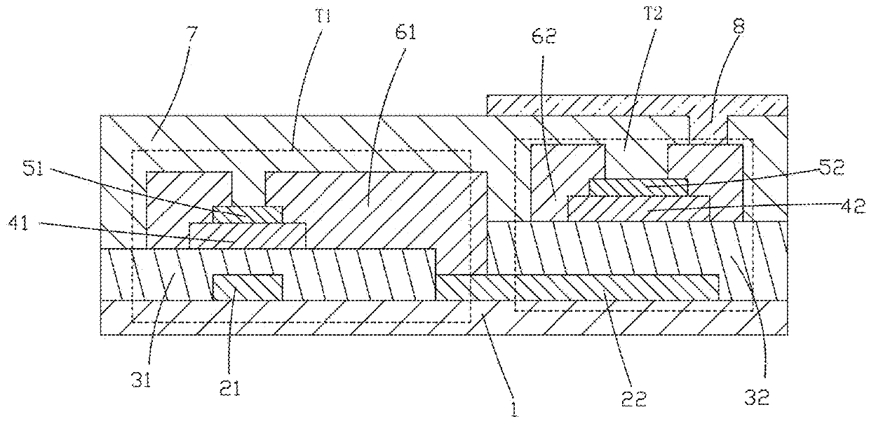
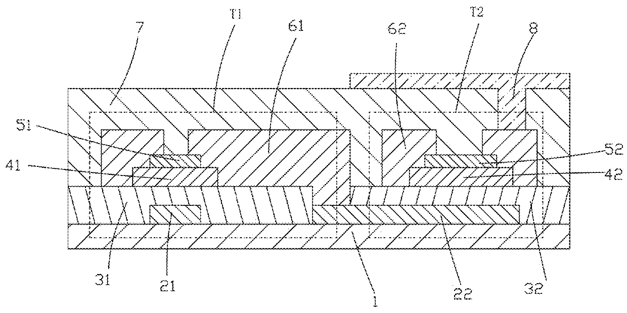
[0049]Referring to FIG. 1, a first embodiment of a thin film transistor (TFT) backplate structure according to the present invention is provided. The TFT backplate structure comprises comprising a substrate 1, a first gate electrode 21 and a second gate electrode 22 on the substrate 1 with a distance in between, a first gate isolation layer 31 on the substrate 1 and the first gate electrode 21, a second gate isolation layer 32 on the substrate 1 and the second gate electrode 22, a first oxide semiconductor layer 41 right over the first gate electrode 21 and on the first gate isolation layer 31, a second oxide semiconductor layer 42 right over the second gate electrode 22 and on the second gate isolation layer 32, a first etching stopper layer 51 on the first oxide semiconductor...


PUM


Abstract

A method is provided for manufacturing a thin film transistor (TFT) backplate that includes a switch TFT and a drive TFT. The method is conducted such that each of the switch TFT and the drive TFT manufactured therewith includes a source electrode / a drain electrode and a gate electrode, and also includes an etching stopper layer, a semiconductor layer, and gate isolation layer that are disposed between the source electrode / the drain electrode and the gate electrode to form a TFT structure. The gate isolation layers of the switch TFT and drive TFT are formed of different materials, such as SiOx and Al2O3, or SiOx and SiNx, or Al2O3 and a mixture of SiNx and SiOx, such that electrical properties of the switch TFT and the drive TFT are made different.

Description

CROSS REFERENCE TO RELATED APPLICATIONS[0001]This is a divisional application of patent application Ser. No. 14 / 426,153, filed on Mar. 4, 2015, which is a national stage of PCT Application Number PCT / CN2014 / 086891, filed on Sep. 19, 2014, claiming foreign priority of Chinese Patent Application Number 201410444171.3, filed on Sep. 2, 2014.FIELD OF THE INVENTION[0002]The present invention relates to a display technology field, and more particularly to a thin film transistor (TFT) backplate structure and a manufacture method thereof.BACKGROUND OF THE INVENTION[0003]A flat panel display possesses advantages of being ultra thin, power saved and radiation free and has been widely utilized. Present flat panel displays mainly comprise a LCD (Liquid Crystal Display) or an OLED (Organic Light Emitting Display).[0004]An organic light emitting diodes display possesses outstanding properties of self-illumination, no required back light, high contrast, being ultra thin, wide view angle, fast resp...

Claims


Application Information

Patent Timeline
Patent Type & Authority Patents(United States)
IPC IPC(8): H01L21/77H01L27/12H01L29/786H01L27/32H01L29/423
CPCH01L27/1237H01L21/77H01L27/12H01L27/127H01L27/1225H01L29/42384H01L29/7869H01L29/78606H01L27/1288H01L2029/42388H01L27/3262H01L29/4908H01L27/124H01L27/1251H10K59/1213
Inventor LV, XIAOWENTSENG, CHIHYUANSU, CHIHYUZHANG, HEJING
Owner TCL CHINA STAR OPTOELECTRONICS TECH CO LTD
Why Eureka
Try Eureka