

Optical waveguide element and optical modulator using the same
a technology of optical modulator and waveguide element, which is applied in the field of optical communication and optical instruments, can solve the problems of low running cost, inability to achieve high-speed modulation, and the drawback of having a length as long as approximately 10 cm, so as to reduce the propagation loss in tm fundamental mode, reduce the coupling to tm fundamental mode, and increase the electro-optical constant
- Summary
- Abstract
- Description
- Claims
- Application Information
AI Technical Summary
Benefits of technology
Problems solved by technology
Method used
Image

Examples
first embodiment
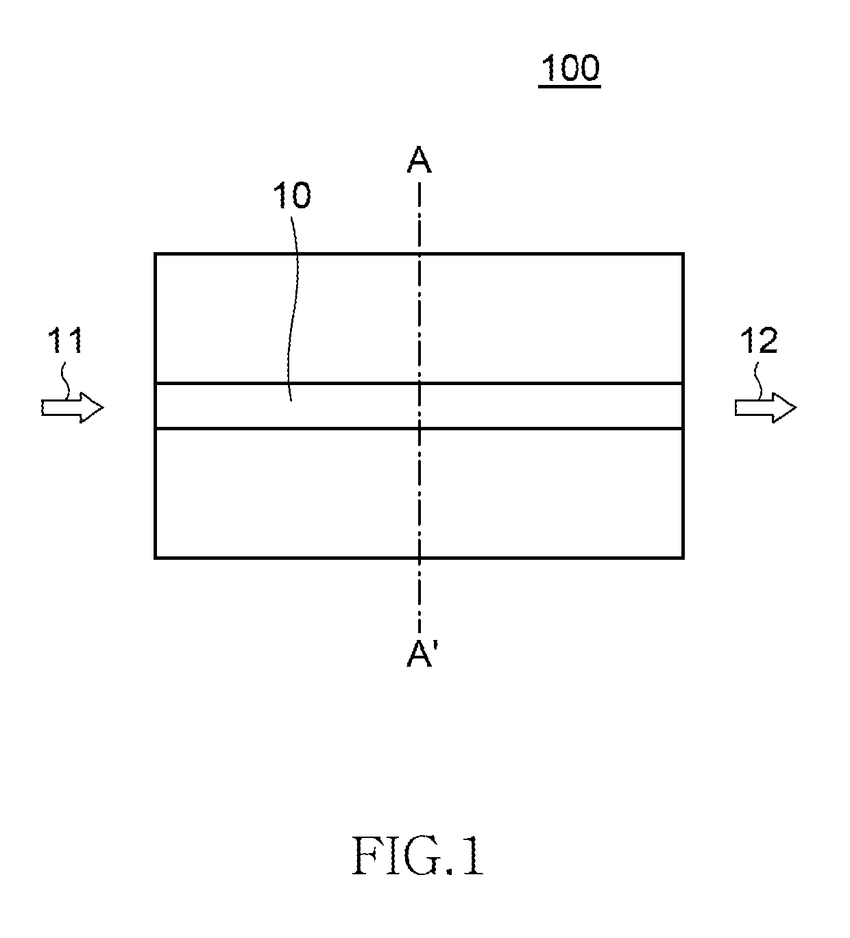
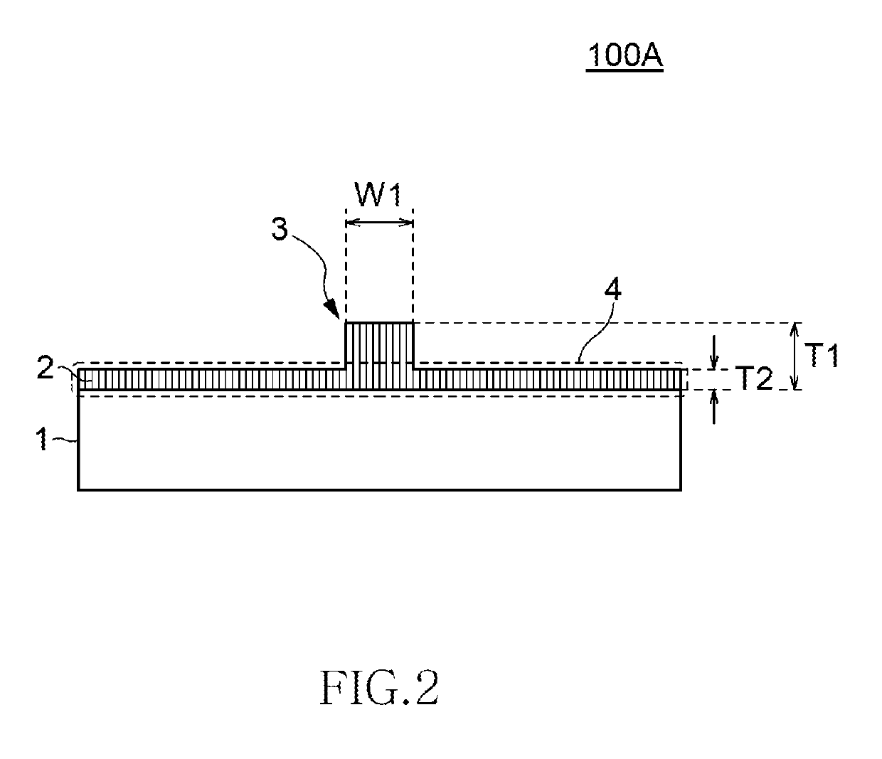
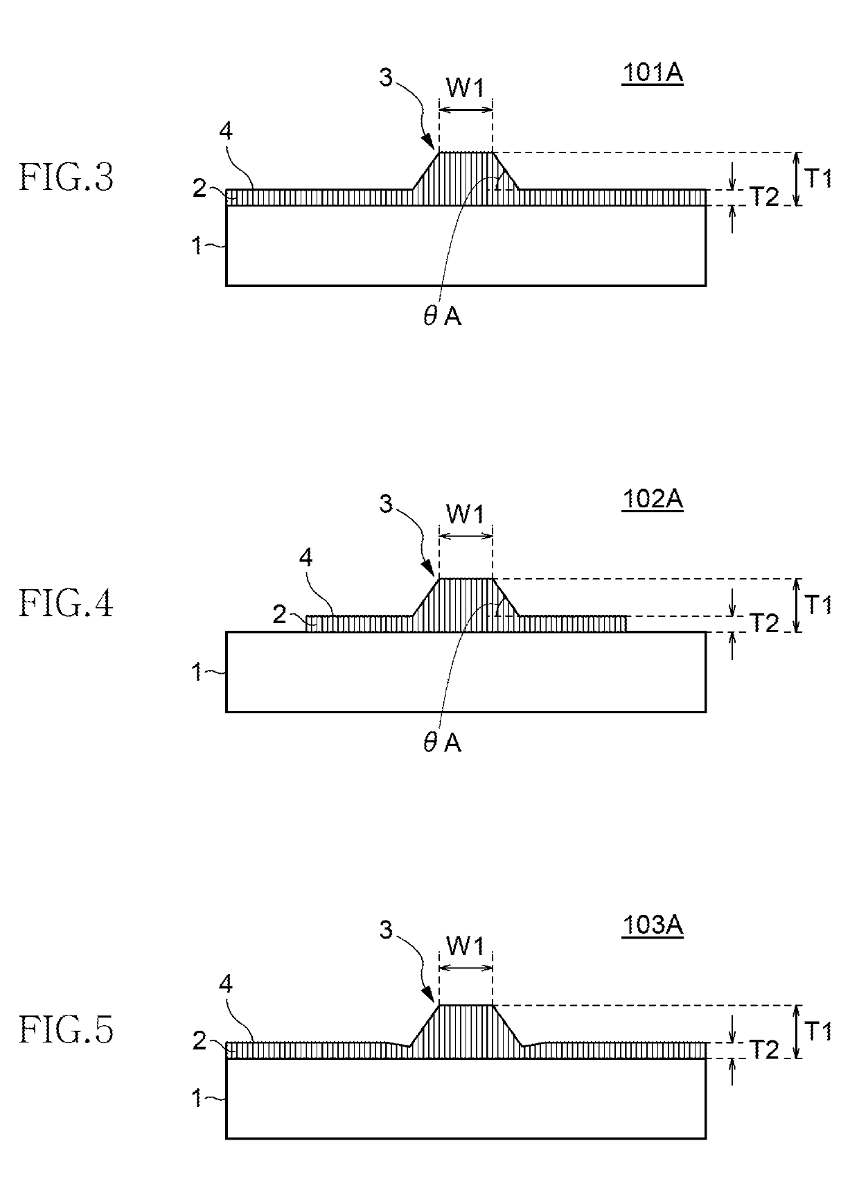
[0059]FIG. 2 is a cross sectional view of the optical waveguide element 100, taken along line A-A′ shown in FIG. 1, and shows the structure of an optical waveguide element 100A according to the first embodiment. The optical waveguide element 100A includes a substrate 1 and a waveguide layer 2 formed on the substrate 1. The waveguide layer 2 has an optical waveguide 10, which has a ridge part 3 having a ridge-shaped cross section. The ridge part 3 is a projection having ridge width W1 and thickness T1. In the optical waveguide element of FIG. 1, the sides of the ridge part 3 are substantially perpendicular to the substrate 1. The waveguide layer 2 further has a slab part 4 having thickness T2, outside a region where the optical waveguide 10 is formed, apart from the ridge part 3. In this embodiment, the slab part 4 includes only a flat layer having a substantially uniform thickness.
[0060]The waveguide layer 2 is made mainly of lithium niobate (LiNbO3). Lithium niobate has a large ele...
second embodiment
[0086]The second embodiment of this invention will now be described.
[0087]FIG. 8 is a sectional view of the optical waveguide element 100B according to the second embodiment of the present invention, taken along line A-A′ shown in FIG. 1. The optical waveguide element 100B differs from the optical waveguide element 100A shown in FIG. 2 according to the first embodiment, in that the slab part 4 includes a flat part 4a and an inclining part 4b. In any other structural respects, the optical waveguide element 100B is identical to the optical waveguide element 100A shown in FIG. 2 according to the first embodiment. Therefore, the components identical to those of the optical waveguide element 100A are designated by the same reference numbers and will not be described repeatedly.
[0088]The flat part 4a of the slab part 4 has thickness that is almost uniform, i.e., thickness T3. The inclining part 4b of the slab part 4 is gradually thinned away from the ridge part 3, and has the maximum thic...
example 1
[0129]Simulation was conducted to see how the effective refractive index N for TE slab mode changes in the optical waveguide element 100A shown in FIG. 2 if the thickness T2 of the slab part 4 is changed. The result of the simulation is shown in FIG. 20. In FIG. 20, Ne is the refractive index the lithium niobate film exhibits to extraordinary light. The actual effective refractive index for the TM fundamental mode is smaller than refractive index Ne depending on the ridge width W or the like. Hence, the threshold value for N / Ne would not be 1.
[0130]As shown in FIG. 20, the effective refractive index N for the TE slab mode decreases as the thickness T2 of the slab part 4 decreases not only in the case where the wavelength is 1550 nm, but also in the case where the wavelength is 633 nm.
PUM
| Property | Measurement | Unit |
|---|---|---|
| length | aaaaa | aaaaa |
| thick | aaaaa | aaaaa |
| inclination angle | aaaaa | aaaaa |
Abstract
Description
Claims
Application Information