Layered structure for an infrared emitter, infrared emitter device and detector

a technology of infrared emitter and layered structure, which is applied in the direction of optical radiation measurement, instruments, spectrophotometry/monochromators, etc., can solve the problems of poor efficiency, low emissivity, and difficult manufacture of optical layered structures suitable for emitter use, so as to reduce the thermal mass of the layered structure, reduce the effective refractive index, and achieve sufficient lossiness

Active Publication Date: 2017-08-15
VAISALA
View PDF11 Cites 5 Cited by
  • Summary
  • Abstract
  • Description
  • Claims
  • Application Information

AI Technical Summary

Benefits of technology

[0020]Compared to the solution according to U.S. Pat. No. 6,177,673, the embodiments of the invention permit, for example, a reduction in the thermal mass of the layered structure. The polycrystalline silicon film of the structure disclosed in the US patent must be made relatively thicker, because the effective refractive index must be reduced, to achieve sufficient lossiness. The manufacture of the structure according to the embodiments of the invention also does not necessarily require the use of ion implantation, making it possible to reduce manufacturing costs. Also in embodiments, in which ion implantation is used, it is possible to reduce the number of ion-implantation stages contained in the manufacturing process with the aid of the embodiments, if this is desired. In addition, the structure according to the invention is more stable at high temperatures.

Problems solved by technology

A drawback with such simple components or surfaces, which are typically manufactured from a single material, is low emissivity and thus poor efficiency.
The manufacture of an optical layered structure suitable for emitter use is, however, very problematical, because the effective emitter use of the component requires a high temperature.
For this reason, most of the known absorber structures are not in practice suitable for emitter use.
The weakness of this construction is that it is difficult to manufacture the semipermeable metal thin film to be the correct thickness, and, in addition, being the outer surface of the detector, it is easily destroyed.
Thus, the structure described in the publication cannot be used as an emitter, as the structure will not withstand the temperatures demanded in emitter use.
The structure also cannot be used in thermal emitters, because metal films like those described do not sufficiently withstand high temperatures.
In addition, a weakness of the structure is that it is extremely difficult to optimize the layer thicknesses according to both thermal and optical demands.
Though the solution described in U.S. Pat. No. 6,177,673 is in many ways progressive and better than those known previously, the emissivity of the structure is unstable at high temperatures.

Method used


Image

  • Layered structure for an infrared emitter, infrared emitter device and detector
  • Layered structure for an infrared emitter, infrared emitter device and detector
  • Layered structure for an infrared emitter, infrared emitter device and detector

Examples


second embodiment

[0076] a detector component is manufactured, which comprises the layered structure described above as well as means connected to the layered structure for measuring the temperature of the layered structure. For example, thermocouples connected in series can be used as temperature measuring means.

third embodiment

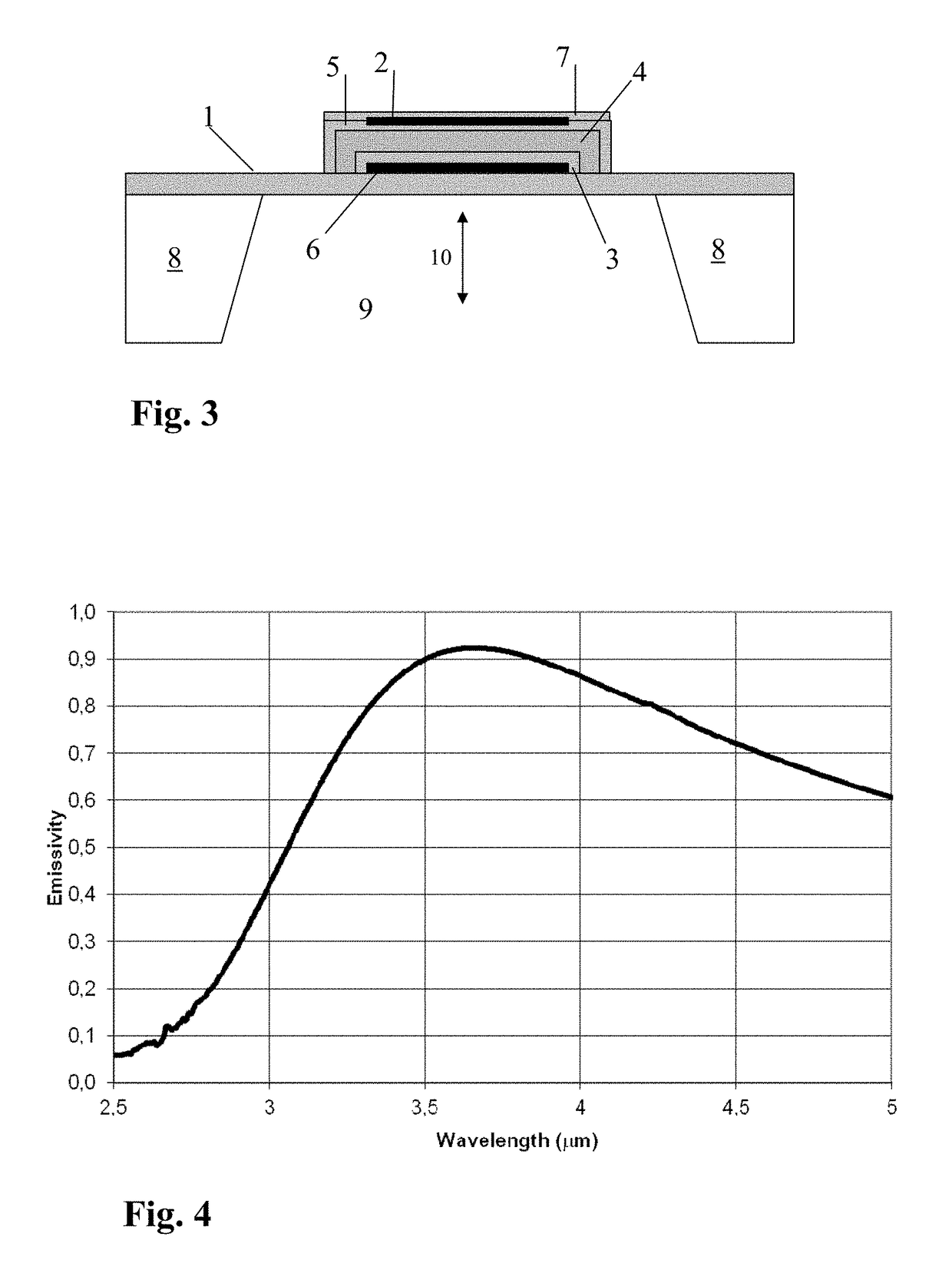
[0077] a filter, i.e. a reflector component is manufactured, which is suitable for reflecting electromagnetic radiation, in such a way that the reflective index changes as a function of the wavelength of the radiation being reflected.

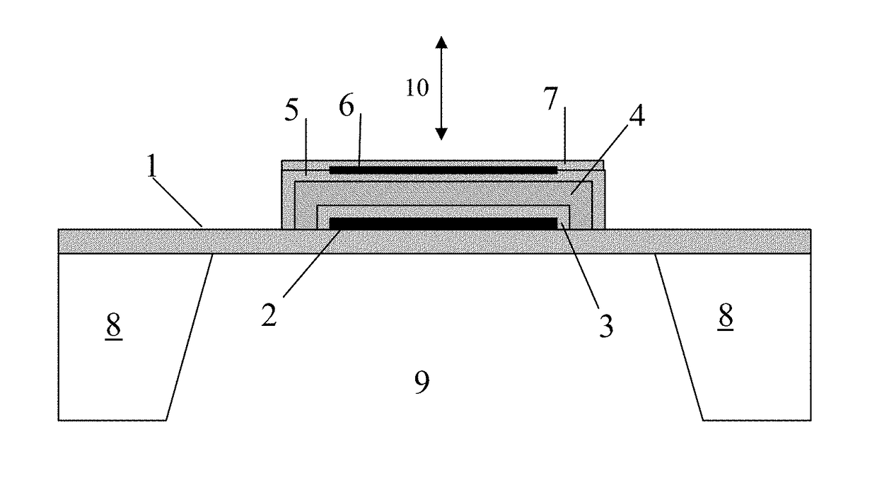
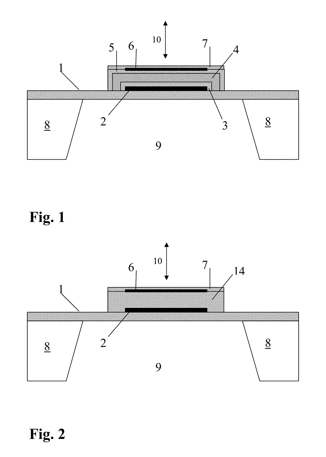
[0078]Within the scope of the invention, solutions deviating from the embodiments can also be envisaged. For example, it is possible to manufacture several intermediate layers 4 and shielding layers 1, 3, 5, and 7 in the layered structure. Several partially transparent layers 6 can also be manufactured, in such a way that these layers are separated to correspond to the example of FIG. 1 or 2 each by its own intermediate layer 3, 4, 5 (FIG. 1), or 14 (FIG. 2).


PUM


Abstract

The present publication describes a heat-resistant optical layered structure, a manufacturing method for a layered structure, and the use of a layered structure as a detector, emitter, and reflecting surface. The layered structure comprises a reflecting layer, an optical structure on top of the reflecting layer, and preferably shielding layers for shielding the reflecting layer and the optical structure. According to the invention, the optical structure on top of the reflecting layer comprises at least one partially transparent layer, which is optically fitted at a distance to the reflecting layer.

Description

FIELD OF TECHNOLOGY[0001]The present invention relates to an optical layered structure according to the preamble to claim 1, suitable for emitter use. The invention also relates to a method for manufacturing an optical layered structure and the use of a layered structure.[0002]Optical structures of this kind are used to emit electromagnetic radiation at a specific wavelength or frequency band. According to the principle of reciprocity, a good emitter is also a good absorber, so that the same optical structure can, suitably adapted, be also used as a detector, which absorbs electromagnetic radiation. In general, the optical structure is thus used to adapt the match the surface of the structure optically to its environment at a desired wavelength range and in a desired manner.[0003]The electromagnetic radiation to be matched to the optical structure is more generally infrared radiation or visible light.[0004]The structure applied to detector and / or emitter use can also be termed optic...

Claims


Application Information

Patent Timeline
Patent Type & Authority Patents(United States)
IPC IPC(8): G02B5/22H01L51/52G01J5/08G01J5/10F21V7/10G01J5/02G01J3/10G01J5/04H05B3/84G01J5/20
CPCG02B5/22F21V7/10G01J3/108G01J5/024G01J5/048G01J5/0809G01J5/10G01J5/20H01L51/529H01L51/5271H05B3/84G01J2005/103H05B2203/013H10K50/856H10K50/87G01J5/0808
Inventor TALVITIE, HANNUKORHONEN, JUKKABLOMBERG, MARTTI
Owner VAISALA
Why Eureka
Try Eureka