
Physically unclonable function (PUF) circuits employing multiple puf memories to decouple a puf challenge input from a puf response output for enhanced security

Inactive Publication Date: 2019-11-07
QUALCOMM INC
View PDF0 Cites 16 Cited by
  • Summary
  • Abstract
  • Description
  • Claims
  • Application Information

AI Technical Summary

Benefits of technology

The patent describes a method for improving the security of a physically unclonable function (PUF) circuit by using multiple PUF memories and intermediate PUF challenge output data words. This decouples the PUF challenge input from the PUF response output, making it difficult to learn and model the PUF circuit. The method includes receiving a PUF challenge input, selecting at least one challenge memory bit cell among a plurality of challenge memory bit cells, and generating a PUF challenge output data word from the selected challenge memory bit cells. The PUF circuit also includes a PUF response memory with a plurality of response memory bit cells, and a means for selecting at least one response memory bit cell and generating a PUF response output data word from the selected response memory bit cells. The technical effect of this method is to enhance the security of the PUF circuit and make it more resistant to machine-learning attacks.

Problems solved by technology

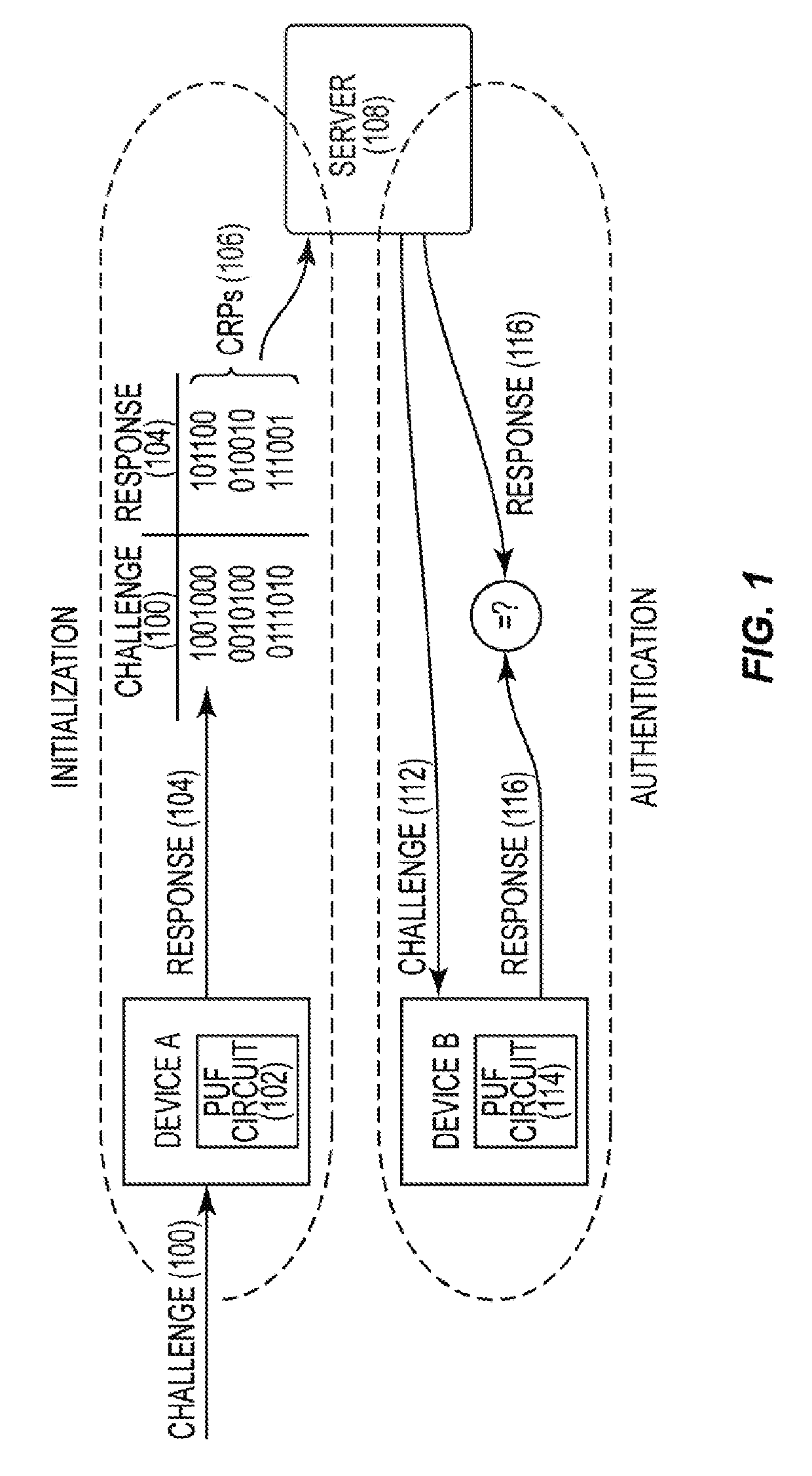
In this manner, it is difficult to discern or learn and model the challenge-response behavior of the PUF circuit, because the PUF challenge input data word into the PUF circuit does not address a memory array that stores memory states representing final logic values in the PUF response output.

Method used


Image

  • Physically unclonable function (PUF) circuits employing multiple puf memories to decouple a puf challenge input from a puf response output for enhanced security
  • Physically unclonable function (PUF) circuits employing multiple puf memories to decouple a puf challenge input from a puf response output for enhanced security
  • Physically unclonable function (PUF) circuits employing multiple puf memories to decouple a puf challenge input from a puf response output for enhanced security

Examples


Embodiment Construction

[0046]With reference now to the drawing figures, several exemplary aspects of the present disclosure are described. The word “exemplary” is used herein to mean “serving as an example, instance, or illustration.” Any aspect described herein as “exemplary” is not necessarily to be construed as preferred or advantageous over other aspects.

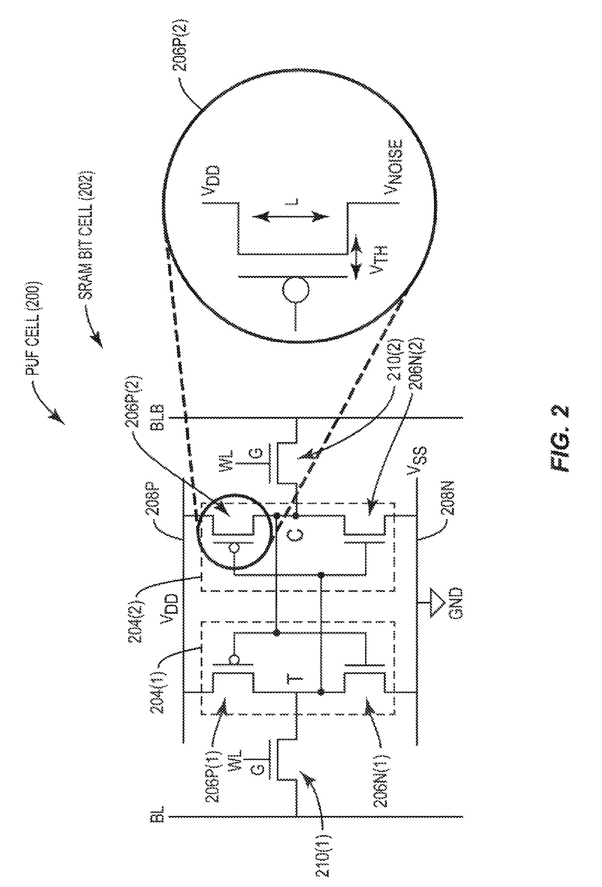
[0047]Aspects disclosed herein include physically unclonable function (PUF) circuits employing multiple PUF memories to decouple a PUF challenge input from a PUF response output for enhanced security. In this regard, in exemplary aspects disclosed herein, a PUF circuit includes a PUF challenge memory as a first PUF memory, and a PUF response memory as a second PUF memory. As a non-limiting example, the PUF challenge memory can be in a first logical PUF layer, and the PUF response memory can be in a second logical PUF layer. A logical PUF layer means a circuit or circuit system having a challenge input and one or more response outputs whose logic value...


PUM


Abstract

Physically unclonable function (PUF) circuits employing multiple PUF memories to decouple a PUF challenge input from a PUF response output for enhanced security. The PUF circuit includes a PUF challenge memory and a PUF response memory. In response to a read operation, the PUF challenge memory uses a received PUF challenge input data word to address PUF challenge memory arrays therein to generate a plurality of intermediate PUF challenge output data words. The PUF response memory is configured to generate a second, final PUF response output data word in response to intermediate PUF challenge output data words. In this manner, it is more difficult to learn the challenge-response behavior of the PUF circuit, because the PUF challenge input data word does not directly address a memory array that stores memory states representing final logic values in the PUF response output data word.

Description

BACKGROUNDI. Field of the Disclosure[0001]The technology of the disclosure relates generally to physically unclonable function (PUF) circuits, and more particularly to a PUF circuit employing a PUF memory array of memory bit cells for generating a PUF response output in response to a challenge input.II. Background[0002]A physical unclonable function (PUF) circuit (sometimes also called a physically unclonable function (PUF)) is a physical entity that is embodied in a physical structure, and is easy to evaluate but hard to predict. A specific challenge and its corresponding response together form a challenge-response pair (CRP) or challenge-response behavior. For example, a response generated by the PUF circuit in response to a challenge may be used to authenticate a device or may be used as a cryptographic key. As another example, a mobile device may include circuitry that is configured to generate a response to a challenge for use as a basis for a device identifier of a device.[000...

Claims


Application Information

Patent Timeline
IPC IPC(8): H04L9/32G11C11/419G11C11/418G06F21/75
CPCG11C11/419G11C11/418G11C11/412G06F21/75H04L9/3278G06F21/73G11C7/24G11C11/417G11C14/0072
Inventor LI, XIAKANG, SEUNG HYUKSTEVENS-YU, NICHOLAS KA MING
Owner QUALCOMM INC
Learn More