Arrayed semiconductor device, optical transmission module, optical module, and method for manufacturing thereof

a semiconductor and optical device technology, applied in semiconductor laser arrangements, semiconductor lasers, lasers, etc., can solve the problems of deterioration of the crystallinity of the mqw layer, the limit of high density mounting considering a space, etc., and achieve the effect of reducing the variation in the performance of semiconductor optical devices

Active Publication Date: 2019-11-14
LUMENTUM JAPAN INC
View PDF0 Cites 1 Cited by
  • Summary
  • Abstract
  • Description
  • Claims
  • Application Information

AI Technical Summary

Benefits of technology

[0011]The present invention has been made in view of such problems and an object of the present invention is to provide an arrayed semiconductor optical device realizing miniaturization of an optical transmitter module and an optical module, and a method for manufacturing thereof while reducing variation in performance of semiconductor optical devices between channels.
[0021]The present invention may provide the arrayed semiconductor optical device realizing miniaturization of the optical transmitter module and the optical module, and the method for manufacturing thereof while reducing variation in performance of semiconductor optical devices between channels.

Problems solved by technology

In this case, since it is necessary to mount each semiconductor optical device individually, there is a limit to high density mounting considering a space required for the mounting.
Additionally, the number of wafers corresponding to the number of channels is fabricated, which is also a problem from a viewpoint of cost reduction.
In the former (lower side grating), a crystallinity of the MQW layer may be deteriorated due to an influence of unevenness of the grating disposed on the lower side of the MQW layer.

Method used


Image

  • Arrayed semiconductor device, optical transmission module, optical module, and method for manufacturing thereof
  • Arrayed semiconductor device, optical transmission module, optical module, and method for manufacturing thereof
  • Arrayed semiconductor device, optical transmission module, optical module, and method for manufacturing thereof

Examples


first embodiment

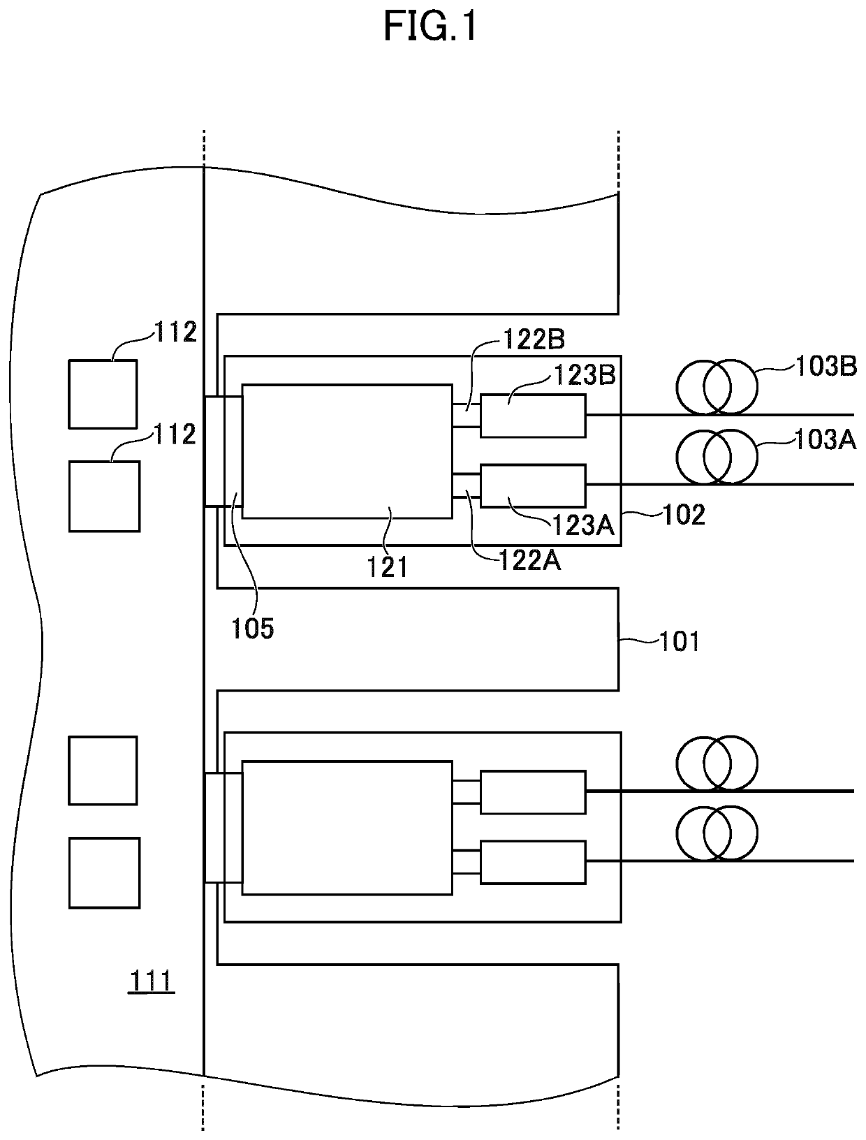
[0033]FIG. 1 is a schematic diagram illustrating a configuration of an optical transmission device 101 according to the first embodiment of the invention. A plurality of optical modules 102 are mounted on the optical transmission device 101. The optical transmission device 101 includes a printed circuit board 111 and an IC 112. The optical transmission device 101 is, for example, a large capacity router or a switch. The optical transmission device 101 has, for example, a function of a signal exchanger and is disposed in a base station or the like. The optical transmission device 101 acquires data for reception (electric signal for reception) from the optical module 102, determines where to send the data using the IC 112 or the like, generates data for transmission (electric signal for transmission), and transmits the data to corresponding optical module 102 through the printed circuit board 111.

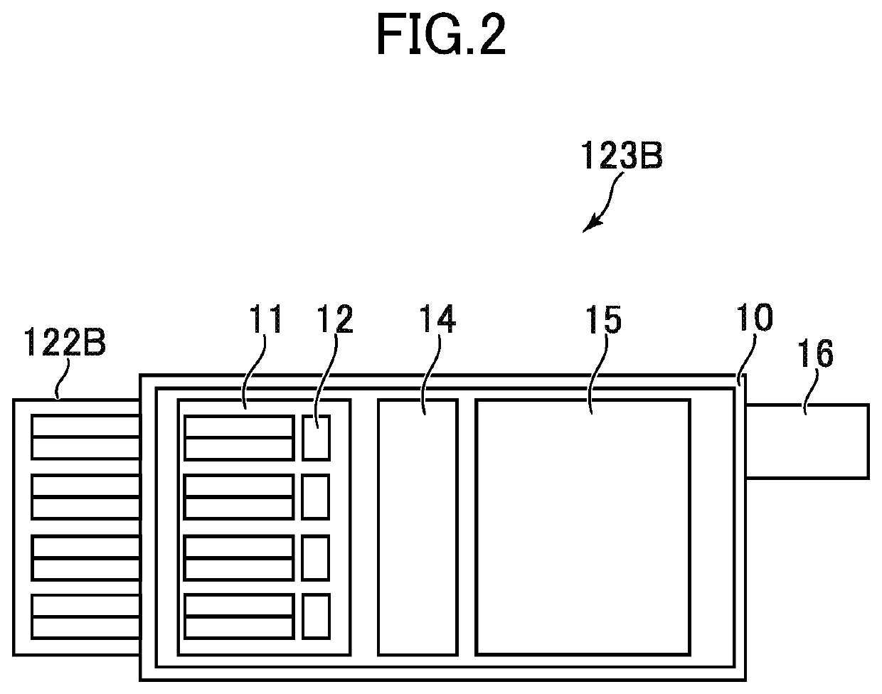
[0034]The optical module 102 is a transceiver having a function of transmission and recep...

second embodiment

[0067]The arrayed semiconductor optical device 11 according to a second embodiment of the present invention is, similarly to the first embodiment, a ridge structure type four-channel multiple wavelength laser device array, and each semiconductor optical device 12 is a semiconductor laser device that outputs a continuous wave (CW), specifically, a DFB laser. A plurality of electro-absorption (EA) modulators that modulate and output the continuous waves from each of the plurality of the semiconductor optical devices 12 are also monolithically integrated into the arrayed semiconductor optical device 11. That is, each semiconductor optical device 12 is a laser portion of the EA modulator integrated DFB laser. The arrayed semiconductor optical device 11 according to the first embodiment includes the Fe-doped InP substrate 20, and the n-side electrode 32 is formed on the same side with respect to the p-side electrode 31 and the semiconductor substrate. On the other hand, the arrayed semic...

third embodiment

[0071]An arrayed semiconductor optical device 11 according to a third embodiment of the invention is, similarly to the first embodiment, a four-channel multiple wavelength laser device array, and each semiconductor optical device 12 is a buried hetero structure type and direct modulation type semiconductor laser device, specifically, a DFB laser. By employing the buried hetero structure type, a semiconductor multilayer structure of semiconductor optical device 12 according to the embodiment is different from that of the first embodiment and a shape of the p-side electrode 31 is also different from that of the first embodiment, but other structures are the same as that of the first embodiment.

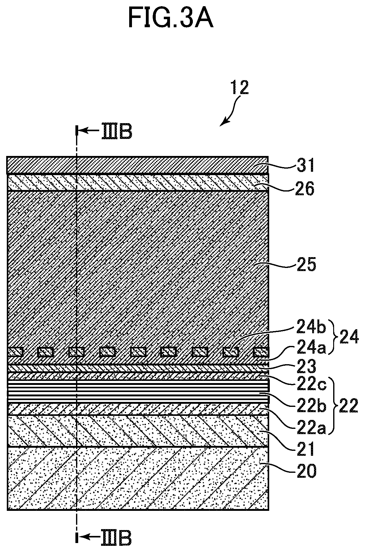
[0072]FIG. 8 is a schematic diagram illustrating a structure of the arrayed semiconductor optical device 11 according to the embodiment. In the semiconductor multilayer structure of the semiconductor optical device 12 according to the embodiment, an n-type InP layer 21, an n-type lower side opti...


PUM


Abstract

In the arrayed semiconductor optical device, a plurality of semiconductor optical devices including a first semiconductor optical device and a second semiconductor optical device are monolithically integrated on a semiconductor substrate, each of the semiconductor optical devices includes a first semiconductor layer having a multiple quantum well layer and a grating layer disposed on an upper side of the first semiconductor layer, a layer thickness of the first semiconductor layer of the first semiconductor optical device is thinner than a layer thickness of the first semiconductor layer of the second semiconductor optical device, and a height of the grating layer of the first semiconductor optical device is lower than a height of the grating layer of the second semiconductor optical device corresponding to difference in the layer thickness of the first semiconductor layer.

Description

CROSS-REFERENCE TO RELATED APPLICATION[0001]The present application is a continuation application of U.S. Ser. No. 15 / 696,604, filed Sep. 6, 2017 which claims priority from Japanese application JP 2016-233431, filed on Nov. 30, 2016, the content of which is hereby incorporated by reference into this application.BACKGROUND OF THE INVENTION1. Field of the Invention[0002]The present invention relates to an arrayed semiconductor optical device, an optical transmitter module, an optical module, and a method for manufacturing thereof, specifically, to a technique for reducing variation in performance of devices between channels.2. Description of the Related Art[0003]An arrayed semiconductor optical device on which a plurality of semiconductor optical devices having mutually different emission wavelengths are mounted is generally used. It is desired to realize both large capacity and small size of the arrayed semiconductor optical device. For such purpose, technique capable of increasing t...

Claims


Application Information

Patent Timeline
Patent Type & Authority Applications(United States)
IPC IPC(8): H01S5/40H01S5/12H01S5/026
CPCH01S5/22H01S5/1231H01S5/4087H01S2304/00H01S5/026H01S5/2272H01S5/02284H01S5/02251
Inventor KITATANI, TAKESHIADACHI, KOICHIRO
Owner LUMENTUM JAPAN INC
Why Eureka
Try Eureka