
Breakdown Layer via Lateral Diffusion

Active Publication Date: 2010-12-02
OVONYX MEMORY TECH LLC
View PDF7 Cites 14 Cited by
  • Summary
  • Abstract
  • Description
  • Claims
  • Application Information

AI Technical Summary

Benefits of technology

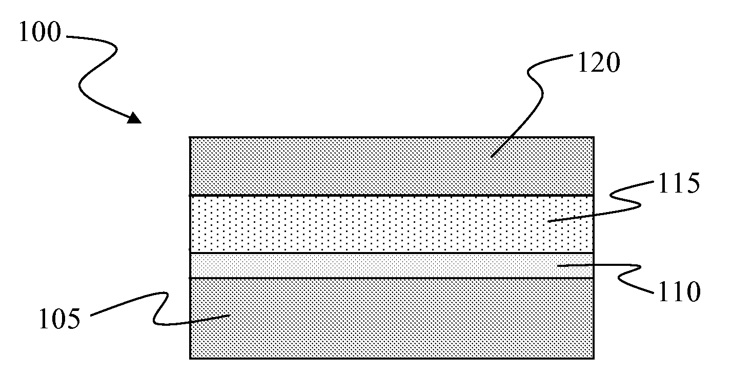
[0016]The presence of the resistivity-enhancing element produces a resistive interface between the variable resistance material and the electrode. Because of the non-uniform concentration profile of the resistivity-enhancing element in the lateral direction, the breakdown resistance of the interface is non-uniform. Specifically, the interfacial breakdown resistance is higher near the lateral edges of the variable resistance material or electrode and decreases toward the interior. This variability in interface breakdown resistance has the effect of biasing the occurrence of the breakdown event toward the interior portion of the interface region. Breakdown is more readily initiated in the lower breakdown resistance interior portions of the interface region than in the higher breakdown resistance lateral portions of the interface region. In effect, the most likely area for electrical breakdown is significantly reduced and is concentrated in a small central region of the device. As a result, the area of the device that is susceptible to localized variations or defects in breakdown layer characteristics is reduced. In addition, this smaller area of most likely breakdown is shifted away from the device edges thereby reducing variations in performance caused by any potential edge effects. The net result is a more consistent breakdown event and greater uniformity in device characteristics.

Problems solved by technology

Because of the non-uniform concentration profile of the resistivity-enhancing element in the lateral direction, the breakdown resistance of the interface is non-uniform.

Method used


Image

  • Breakdown Layer via Lateral Diffusion
  • Breakdown Layer via Lateral Diffusion
  • Breakdown Layer via Lateral Diffusion

Examples


Embodiment Construction

[0027]Although this invention will be described in terms of certain preferred embodiments, other embodiments that are apparent to those of ordinary skill in the art, including embodiments that do not provide all of the benefits and features set forth herein, are also within the scope of this invention. Accordingly, the scope of the invention is defined only by reference to the appended claims.

[0028]This invention provides variable resistance memory devices designed to operate with reduced programming currents. The programming current provides the energy needed to induce changes between the resistance states of the active variable resistance memory material of the device. In order to reduce power consumption, it is desirable to minimize the programming current. In this invention, reduction in programming current is achieved by using a breakdown layer to reduce the area of contact between the electrode delivering the programming current and the active variable resistance material. As ...


PUM

PropertyMeasurementUnit
Thicknessaaaaaaaaaa
Concentrationaaaaaaaaaa
Electrical resistanceaaaaaaaaaa

Abstract

An electronic device including a breakdown layer having variable thickness. The device includes a variable resistance material positioned between two electrodes. A breakdown layer is interposed between the variable resistance material and one of the electrodes. The breakdown layer has a non-uniform thickness, which serves to bias the breakdown event toward the thinner portions of the breakdown layer. As a result, the placement, size, and number of ruptures in the breakdown layer are more consistent over a series or array of devices. The variable resistance material may be a phase-change material. The variable-thickness breakdown layer may be formed through a diffusion process by introducing a gas containing a resistivity-enhancing species to the environment of segmented variable resistance devices during fabrication. The resistivity-enhancing element penetrates the outer perimeter of the variable resistance material and diffuses toward the interior of the device. The resistivity-enhancing species increases the resistance of the interface between the variable resistance material and the electrode by interacting with the variable resistance material and / or electrode to form a resistive interfacial material. Based on the diffusional nature of the process, the concentration of the resistivity-enhancing species decreases toward the center of the device and as a result, the breakdown layer is thinner toward the center of the device.

Description

FIELD OF INVENTION[0001]This invention relates to variable resistance memory devices. More particularly, this invention relates to a device structure and methods of making variable resistance memory devices having reduced programming currents. Most particularly, this invention relates to a variable resistance memory device structure that includes a breakdown layer formed through a lateral diffusion process.BACKGROUND OF THE INVENTION[0002]Variable resistance materials are promising active materials for next-generation electronic storage and computing devices. A variable resistance material possesses two or more states that differ in electrical resistance and can be programmed back and forth between the states by providing energy to induce an internal chemical, electronic, or physical transformation of the material that manifests itself as a change in resistance of the material. The different resistance states can be associated with different data values and used as memory states to ...

Claims


Application Information

Patent Timeline
IPC IPC(8): H01C7/00H01C17/00
CPCG11C13/0004H01C7/006H01C17/08H01L45/06H01L45/12Y10T29/49082H01L45/143H01L45/144H01L45/148H01L45/1658H01L45/1683H01L45/1246H10N70/801H10N70/828H10N70/231H10N70/8825H10N70/884H10N70/046H10N70/8828H10N70/066
Inventor CZUBATYJ, WOLODYMYRLOWREY, TYLERSPALL, EDWARD J.
Owner OVONYX MEMORY TECH LLC
Learn More