Eureka AIR delivers breakthrough ideas for toughest innovation challenges, trusted by R&D personnel around the world.

Target selection improvements for better design alignment

Active Publication Date: 2019-11-28
KLA TENCOR CORP
View PDF4 Cites 1 Cited by
  • Summary
  • Abstract
  • Description
  • Claims
  • Application Information

AI Technical Summary

Benefits of technology

The patent describes a method of evaluating a pattern-to-design alignment target in an image frame of a die on a wafer. The method involves receiving a hotspot location and biasing pattern-to-design alignment targets in the image frame to include the hotspot location. The alignment targets are then evaluated for repetitive patterns. In one embodiment, the image frame is divided into regularly-sized blocks and the evaluation includes generating X and Y projections, sampling a plurality of points with a highest gradient in both X and Y, creating target locations at a cross-section of the points, and evaluating uniqueness of the points. The method can also include filtering the image frame with adaptive Fourier filtering and selecting points with maximum intensity as the alignment targets. The technical effect of the patent is to improve the accuracy and efficiency of evaluating pattern-to-design alignment targets in image frames.

Problems solved by technology

However, as the dimensions of semiconductor devices decrease, inspection becomes even more important to the successful manufacture of acceptable semiconductor devices because smaller defects can cause the devices to fail.
For instance, as the dimensions of semiconductor devices decrease, detection of defects of decreasing size has become necessary since even relatively small defects may cause unwanted aberrations in the semiconductor devices.
As design rules shrink, however, semiconductor manufacturing processes may be operating closer to the limitation on the performance capability of the processes.
In addition, smaller defects can have an impact on the electrical parameters of the device as the design rules shrink, which drives more sensitive inspections.
As design rules shrink, the population of potentially yield-relevant defects detected by inspection grows dramatically, and the population of nuisance defects detected by inspection also increases dramatically.
Therefore, more defects may be detected on the wafers, and correcting the processes to eliminate all of the defects may be difficult and expensive.
Furthermore, at smaller design rules, process-induced failures, in some cases, tend to be systematic.
That is, process-induced failures tend to fail at predetermined design patterns often repeated many times within the design.
The interactions among the wafer printing process, wafer pattern, and inspection system is extremely complicated.
These problems make image rendering the most difficult task in PDA.
Thus, the PDA quality at logic care areas in not sufficient.
Care area expansion can occur due to system specifications for placement accuracy or can occur due to PDA alignment errors.
PDA targets, then hotspots may not be inspected or the PDA targets may not be selected to provide the best inspection.
It is cost-prohibitive to select an entire image frame as a PDA area.
As seen in FIG. 3, this results in increased care area expansion due to PDA alignment errors and possible loss of sensitivity to key defects of interest.

Method used


Image

  • Target selection improvements for better design alignment
  • Target selection improvements for better design alignment
  • Target selection improvements for better design alignment

Examples


Embodiment Construction

[0038]Although claimed subject matter will be described in terms of certain embodiments, other embodiments, including embodiments that do not provide all of the benefits and features set forth herein, are also within the scope of this disclosure. Various structural, logical, process step, and electronic changes may be made without departing from the scope of the disclosure. Accordingly, the scope of the disclosure is defined only by reference to the appended claims.

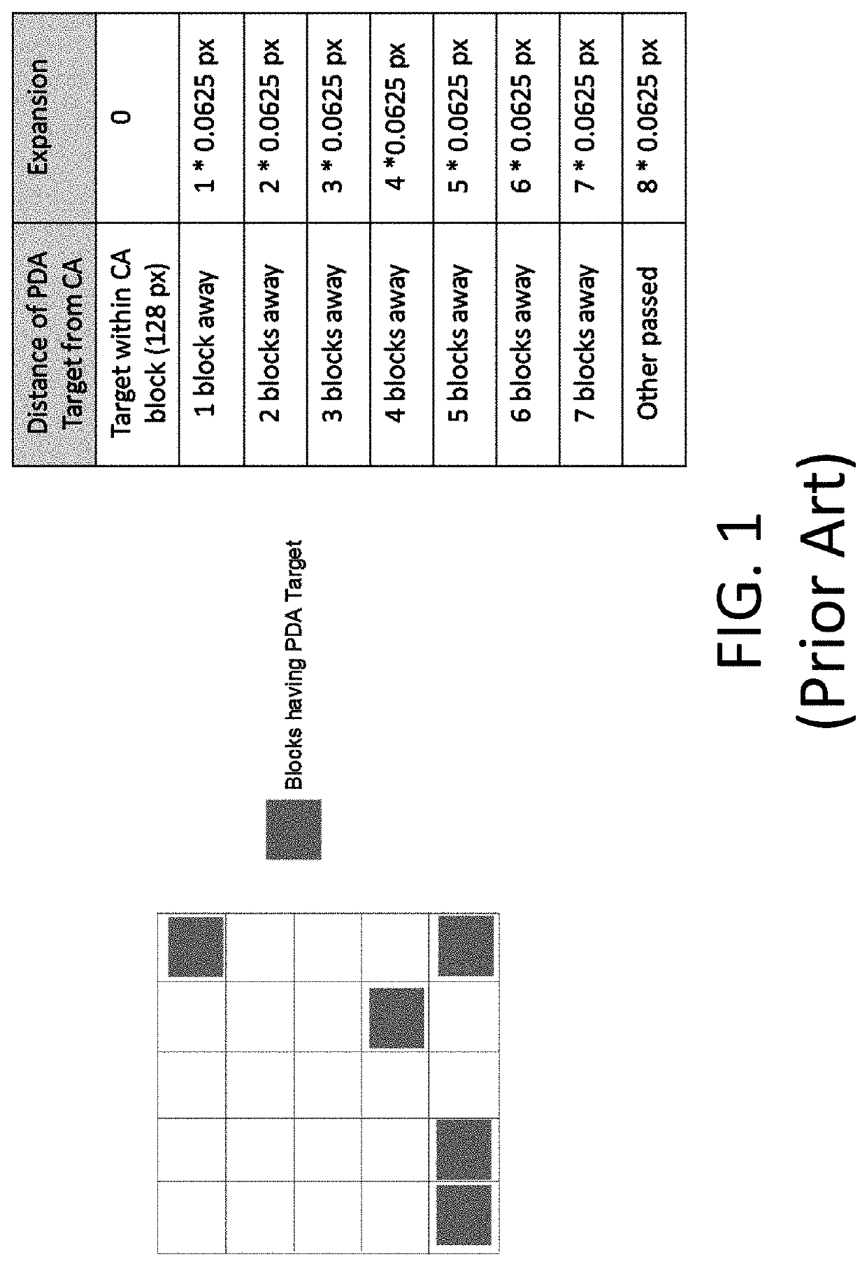
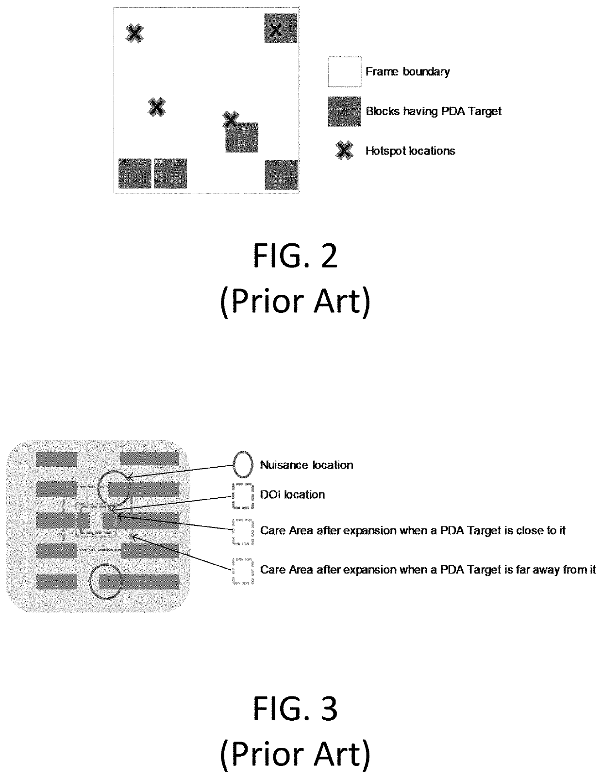
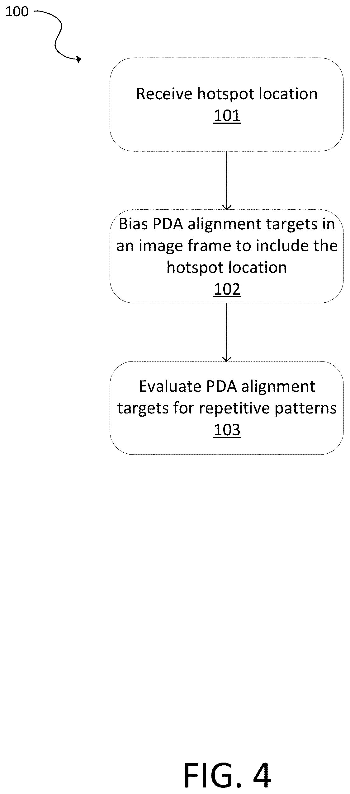
[0039]Embodiments disclosed herein can achieve more accurate design alignment to an image by improved PDA target selection strategies. Better design alignment can provide better care area position accuracy, which can help provide improved sensitivity and nuisance suppression. Better design alignment also can provide tighter care area borders, which can reduce nuisance and improve sensitivity. Better targets for alignment can provide higher defect location accuracy and correct binning in design.

[0040]In the embodiments dis...


PUM


Abstract

Techniques and systems to achieve more accurate design alignment to an image by improved pixel-to-design alignment (PDA) target selection are disclosed. PDA targets in an image frame of a die can be biased to include a hotspot location in one of the PDA targets. The PDA targets can be evaluated for repetitive patterns by analyzing the uniqueness of the points used as the PDA targets.

Description

CROSS-REFERENCE TO RELATED APPLICATIONS[0001]This application claims priority to the provisional patent application filed May 22, 2018 and assigned U.S. App. No. 62 / 675126, the disclosure of which is hereby incorporated by reference.FIELD OF THE DISCLOSURE[0002]This disclosure relates to inspection of semiconductor wafers.BACKGROUND OF THE DISCLOSURE[0003]Evolution of the semiconductor manufacturing industry is placing ever greater demands on yield management and, in particular, on metrology and inspection systems. Critical dimensions continue to shrink, yet the industry needs to decrease time for achieving high-yield, high-value production. Minimizing the total time from detecting a yield problem to fixing it determines the return-on-investment for a semiconductor manufacturer.[0004]Fabricating semiconductor devices, such as logic and memory devices, typically includes processing a semiconductor wafer using a large number of fabrication processes to form various features and multip...

Claims


Application Information

Patent Timeline
IPC IPC(8): G06T7/00G01N23/2251
CPCG06T2207/20021G06T2207/30148G06T2207/10061G06T7/0006G01N23/2251G01N2223/6116H01L22/12H01L22/26H01L22/30H01L21/67242H01L21/027
Inventor KUMAR, SANTOSHPERALI, PAVAN KUMAR
Owner KLA TENCOR CORP
Why Eureka
Eureka Blog
Learn More