Goa circuit and OLED display device

a technology of oled display device and gate driver, which is applied in the field of display techniques, can solve the problems of degrading the display quality of the oled display device, complex circuit, and large number of thin film transistors and capacitors, and achieves the effects of simplifying the circuit structure, facilitating narrow-border display, and reducing the number of tfts and capacitors

Active Publication Date: 2019-12-12
WUHAN CHINA STAR OPTOELECTRONICS SEMICON DISPLAY TECH CO LTD
View PDF6 Cites 1 Cited by
  • Summary
  • Abstract
  • Description
  • Claims
  • Application Information

AI Technical Summary

Benefits of technology

[0072]The present invention provides the following advantages. The present invention provides a GOA circuit, comprising: a plurality of cascaded GOA units, each GOA unit comprising a scan signal output module and an emitting signal output module electrically connected to the scan signal output module; during a frame period, the scan signal output module is capable of outputting a scanning signal including at least two low potential pulses within a frame time, and the light emitting signal output module can output a valid emitting signal according to the scan signal outputted by the scan signal output module. Thus, the GOA circuit for scan signal and the GOA circuit for emitting signal in the conventional design are integrated into a GOA circuit, which can reduce the number of TFTs and capacitors, simplify the circuit structure, and facilitate narrow-border display. The present invention also provides an OLED display device, with a GOA circuit capable of outputting a scan signal and an emitting signal at the same time, and the circuit structure is simple and is conducive to the realization of a narrow-border display.

Problems solved by technology

During the use, due to the aging of the OLED and the threshold voltage drift of the driving TFT, the display quality of the OLED display device is degraded.
In the traditional mode, the EM GOA circuit and the SCAN GOA circuit are respectively disposed to generate the EM signal and the SCAN signal, resulting in the complex circuit, large number of thin film transistors and capacitors, which is not conducive to the realization of narrow borders.

Method used


Image

  • Goa circuit and OLED display device
  • Goa circuit and OLED display device
  • Goa circuit and OLED display device

Examples


Embodiment Construction

[0077]To further explain the technique means and effect of the present invention, the following uses preferred embodiments and drawings for detailed description.

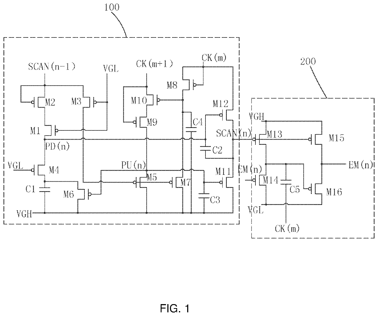
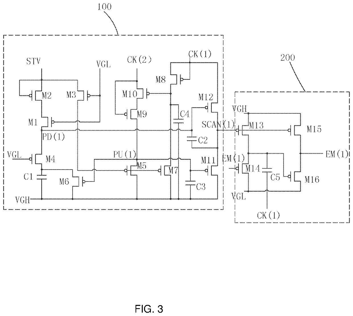
[0078]Referring to FIG. 1, the present invention provides a GOA circuit, which comprises: a plurality of cascaded GOA units, with each GOA unit comprising: a scan signal output module 100 and an emitting signal output module 200 electrically connected to the scan signal output module 100.

[0079]For a positive integer n, except the first GOA unit, in the n-th GOA unit:

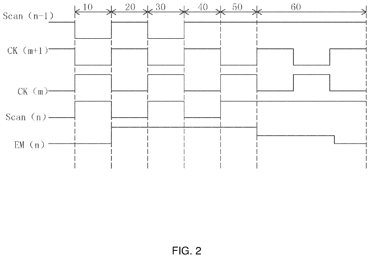
[0080]The scan signal output module 100, receiving an m-th clock signal CK(m), an (m+1)-th clock signal CK(m+1), and a scan signal SCAN(n−1) of the (n−1)-th GOA unit, is for outputting a scan signal SCAN(n) of n-th GOA unit to sub-pixels of n-th row and the emitting signal output module 200 of the n-th GOA unit according to the m-th clock signal CK(m) under the control of the scan signal of the (n−1)-th GOA unit SCAN(n−1);

[0081]the emitting signal output module 2...


PUM


Abstract

The invention provides a GOA circuit and OLED display device. The GOA circuit comprises a plurality of cascaded GOA units, with each GOA unit comprising: a scan signal output module and an emitting signal output module electrically connected to the scan signal output module; during a frame period, the scan signal output module is capable of outputting a scanning signal including at least two low potential pulses within a frame time, and the light emitting signal output module can output a valid emitting signal according to the scan signal outputted by the scan signal output module. Thus, the GOA circuit for scan signal and the GOA circuit for emitting signal in the conventional design are integrated into a GOA circuit, which can reduce the number of TFTs and capacitors, simplify the circuit structure, and facilitate narrow-border display.

Description

BACKGROUND OF THE INVENTION1. Field of the Invention[0001]The present invention relates to the field of display techniques, and in particular to a gate driver on array (GOA) circuit and an light-emitting diode (OLED) display device.2. The Related Arts[0002]The organic light-emitting diode (OLED) display device provides the advantages of self-luminous, low driving voltage, high luminous efficiency, short response time, sharpness and contrast, nearly 180° viewing angle, wide temperature range, flexibility, ability to achieve flexible display and large-area full-color display, and many other advantages, and is recognized by the industry as the most promising display device.[0003]The OLED display device generally comprises a substrate, an anode disposed on the substrate, a hole injection layer (HIL) disposed on the anode, a hole transport layer (HTL) disposed on the hole injection layer, a light-emitting layer disposed on the hole transport layer, an electron transport layer (ETL) on th...

Claims


Application Information

Patent Timeline
Patent Type & Authority Applications(United States)
IPC IPC(8): G09G3/3266G09G3/3258
CPCG09G2310/08G09G2380/02G09G3/3258G09G2300/0408G09G3/3266G09G3/3208G09G3/3674G09G2300/0861G09G2310/0286
Inventor LIU, JIE
Owner WUHAN CHINA STAR OPTOELECTRONICS SEMICON DISPLAY TECH CO LTD
Why Eureka
Try Eureka