Light emitting diode display apparatus and manufacturing method thereof

a technology of light-emitting diodes and display apparatuses, which is applied in the direction of electrical apparatus, basic electric elements, and semiconductor devices, can solve the problems of difficult mass transfer, poor mass transfer yield, and many problems of miniaturized light-emitting diodes as displays, and achieves the goal of improving the mass transfer yield and wide color gamut color specifications

Active Publication Date: 2020-03-12
AU OPTRONICS CORP
View PDF0 Cites 1 Cited by
  • Summary
  • Abstract
  • Description
  • Claims
  • Application Information

AI Technical Summary

Benefits of technology

[0008]The light emitting diode display apparatus according to one of the aforementioned embodiments can provide a wide color gamut color specification.
[0009]

Problems solved by technology

However, the application of miniaturized light emitting diodes as displays still faces many problems.
In particular, in the process of mass transfer of lig

Method used


Image

  • Light emitting diode display apparatus and manufacturing method thereof
  • Light emitting diode display apparatus and manufacturing method thereof
  • Light emitting diode display apparatus and manufacturing method thereof

Examples


Embodiment Construction

[0019]In the following detailed description, for purposes of explanation, numerous specific details are set forth in order to provide a thorough understanding of the disclosed embodiments. It will be apparent, however, that one or more embodiments may be practiced without these specific details. In other instances, well-known structures and devices are schematically shown in order to simplify the drawing.

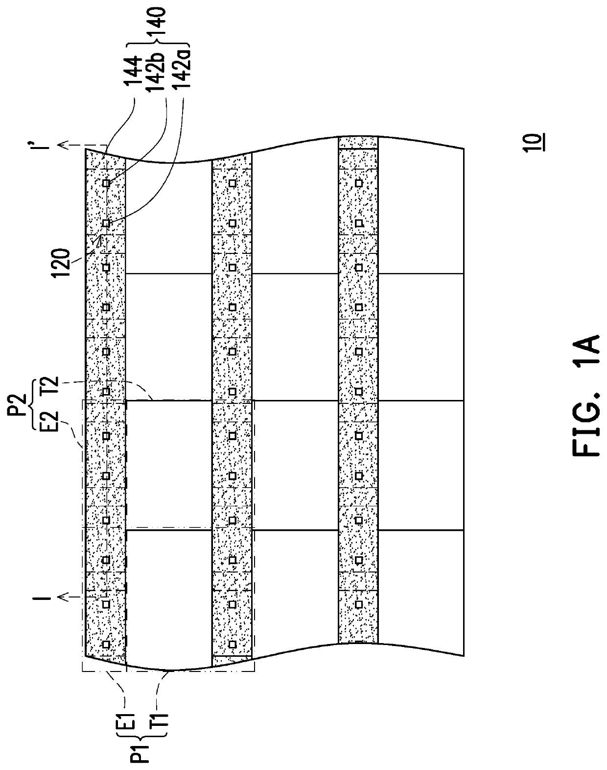
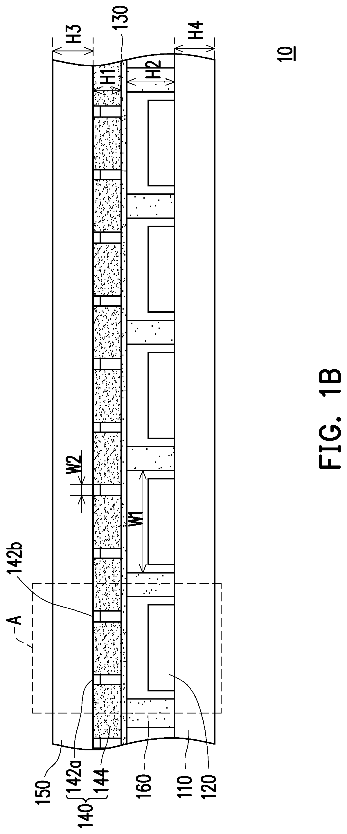
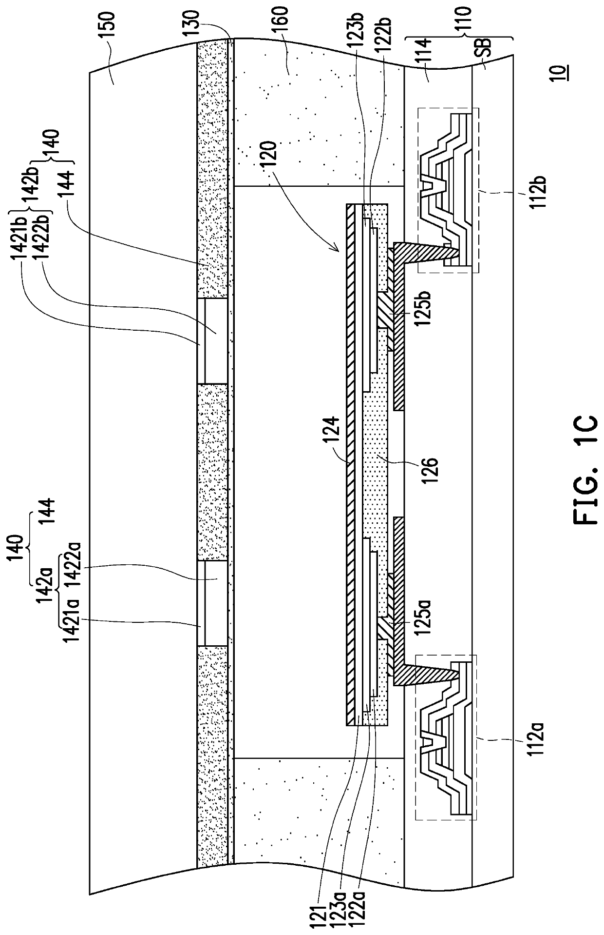
[0020]FIG. 1A is a schematic top view illustrating a light emitting diode display apparatus according to an embodiment of the invention. FIG. 1B is a schematic cross-sectional view illustrating the light emitting diode display apparatus of FIG. 1A along an I-I′ section line. FIG. 1C is an enlarged view illustrating an area A of FIG. 1B. For convenience of description, an adhesive layer 130 and a second substrate 150 of a light emitting diode display apparatus 10 in FIG. 1A are omitted.

[0021]Referring to FIG. 1A to FIG. 1C, the light emitting diode display apparatus 10 of the present...


PUM


Abstract

The light emitting diode display apparatus including a first substrate, a plurality of light emitting diodes, an adhesive layer, a color layer, and a second substrate is provided. The first substrate has a plurality of switching elements. The light emitting diode includes a first semiconductor layer, a plurality of second semiconductor layers, a plurality of light emitting layers, a first electrode, and a plurality of second electrodes. The first electrode is disposed on the first semiconductor layer. The second electrodes are respectively disposed on the corresponding second semiconductor layers. Each of the second electrodes is electrically connected to the corresponding switching element. The adhesive layer and the first substrate are respectively located at two opposite sides of the light emitting diode. The color layer is disposed on the first substrate and covers the adhesive layer and the light emitting diode. The second substrate is disposed opposite to the first substrate.

Description

CROSS REFERENCE TO RELATED APPLICATION[0001]This application claims the priority benefit of Taiwan application serial no. 107131885, filed on Sep. 11, 2018. The entirety of the above-mentioned patent application is hereby incorporated by reference herein and made a part of specification.BACKGROUND OF THE INVENTIONField of the Invention[0002]The invention relates to a display apparatus, and particularly relates to a light emitting diode display apparatus.Description of Related Art[0003]Although the mainstream displays on the market are liquid crystal displays and organic light emitting diode displays, with the progress of science and technology, the size of many photoelectric elements has gradually grown to miniaturization. After miniaturization, the light emitting diode, as a backlight source of the liquid crystal display, can be partitioned into smaller units and can operate its light and dark. Therefore, the miniaturized light emitting diode can be applied to high dynamic range (H...

Claims


Application Information

Patent Timeline
IPC IPC(8): H01L25/18H01L27/15H01L33/38H01L33/62H01L33/50H01L33/52H01L33/00H01L25/00
CPCH01L33/52H01L33/38H01L27/15H01L33/62H01L25/50H01L33/0079H01L2933/0041H01L33/505H01L25/18H01L27/156H01L25/0753H01L25/167H01L27/153H01L33/20H01L33/44H01L33/502H01L33/507H01L33/08H01L33/0093
Inventor WU, YANG-ENSU, SUNG-YU
Owner AU OPTRONICS CORP
Why Eureka
Try Eureka