
Organic Light Emitting Display Device and Pixel Sensing Method of the Same

Active Publication Date: 2020-06-25
LG DISPLAY CO LTD
View PDF0 Cites 10 Cited by
  • Summary
  • Abstract
  • Description
  • Claims
  • Application Information

AI Technical Summary

Benefits of technology

The patent is for a new kind of display that reduces common noise and improves the accuracy and reliability of sensing its pixels. This means that the display can better control the brightness and color of each pixel, resulting in a better overall performance.

Problems solved by technology

However, due to various causes such as process properties, time varying properties and the like, the driving characteristics become different among the pixels.
Such a difference in driving characteristic causes a luminance deviation, which is a limitation in displaying image as desired quality.
So, common noise of the display panel may be reflected on the pixel current sensed through the current integrator.
The common noise of the panel may be caused by various causes such as process characteristics, driving environment, etc., and may affect respective sensing channels in different sizes.
This common noise is amplified by an integral amplifier to distort the integral output voltage, so that sensing results may vary between current integrators even when sensing a same pixel current.

Method used


Image

  • Organic Light Emitting Display Device and Pixel Sensing Method of the Same
  • Organic Light Emitting Display Device and Pixel Sensing Method of the Same
  • Organic Light Emitting Display Device and Pixel Sensing Method of the Same

Examples


Embodiment Construction

[0042]The advantages and features of the present disclosure and methods of accomplishing the same may be understood more readily by reference to the following detailed descriptions of exemplary embodiments and the accompanying drawings. The present disclosure may, however, be embodied in many different forms and should not be construed as being limited to the exemplary embodiments set forth herein. Rather, these exemplary embodiments are provided so that this disclosure will be thorough and complete and will fully convey the concept of the present disclosure to those skilled in the art, and the present disclosure is defined by the appended claims.

[0043]The shapes, sizes, percentages, angles, numbers, etc. shown in the figures to describe the exemplary embodiments of the present disclosure are merely examples and not limited to those shown in the figures. Like reference numerals denote like elements throughout the specification. When the terms ‘comprise’, ‘have’, ‘consist of’ and the...


PUM


Abstract

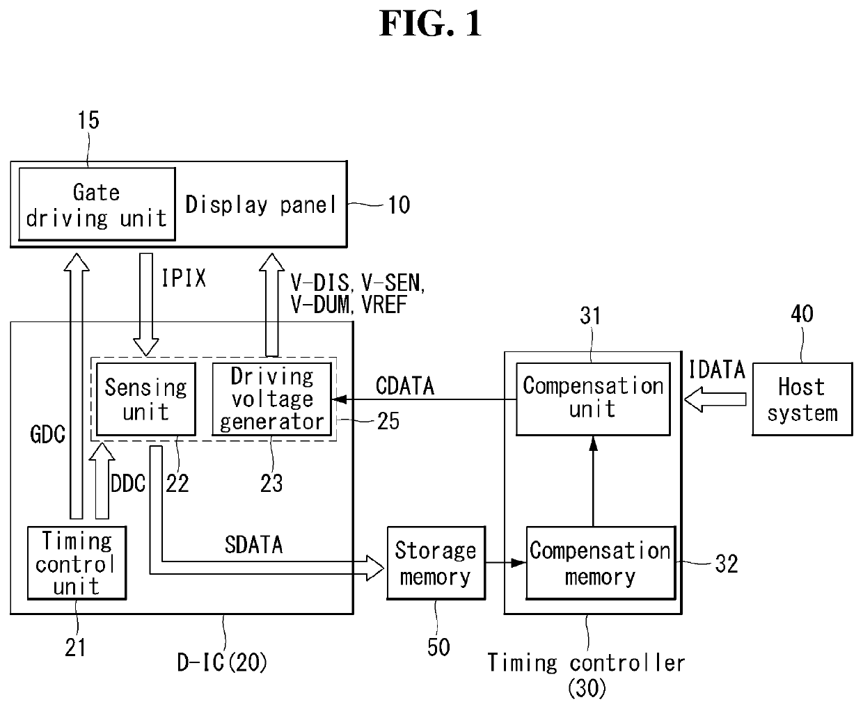
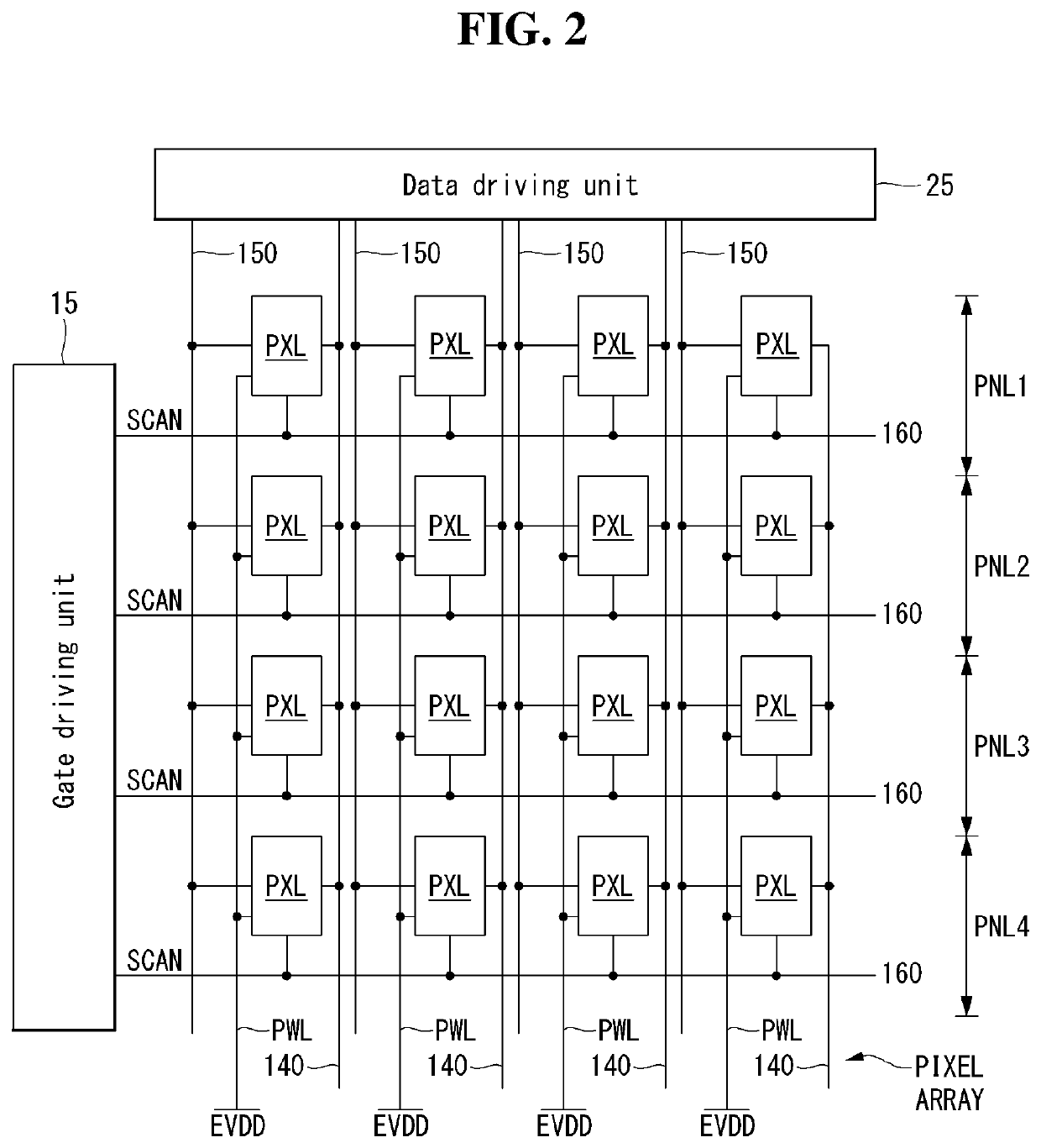
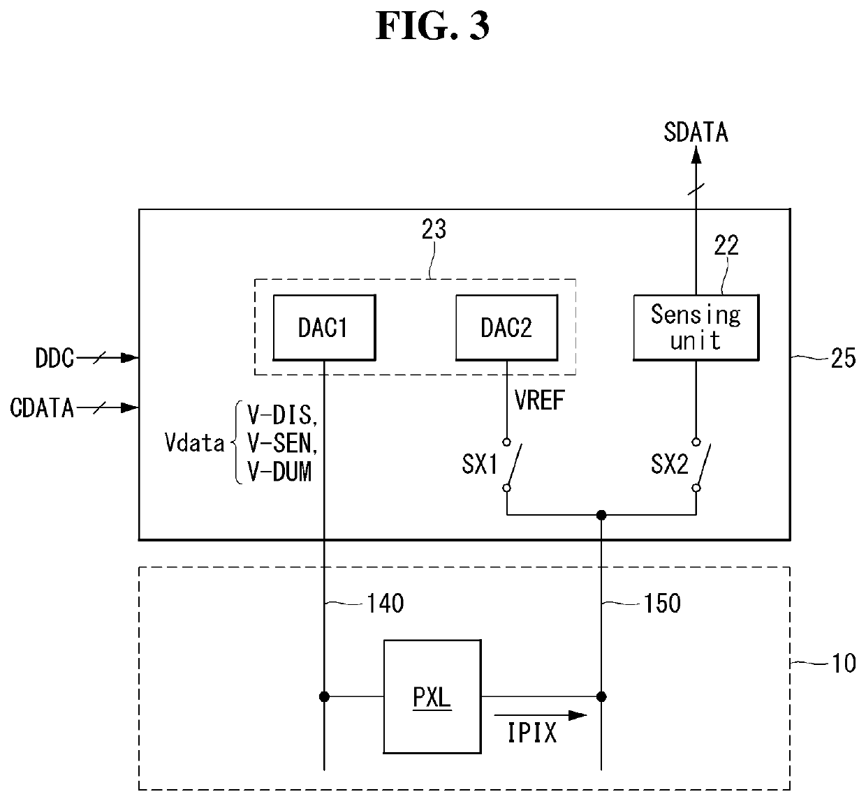
A display device includes a display panel, a driving circuit, a sensing circuit, and a compensation circuit. The display panel includes a first pixel and a second pixel. The driving circuit provides a preset sensing voltage to the first pixel of the display panel, and provides a dummy voltage to the second pixel of the display panel. A first channel of a sensing circuit generates a first integrated voltage signal indicative of a magnitude of a first pixel current generated by the first pixel. A second channel of the sensing circuit generates a second integrated voltage signal indicative of a magnitude of a first dummy current generated by the second pixel. The compensation circuit determines a compensation amount from a difference between an output of the first and second channels of the sensing circuit, and compensates a display voltage of the first pixel by the compensation amount.

Description

CROSS REFERENCE TO RELATED APPLICATIONS[0001]This application claims the benefit of Korea Patent Application No. 10-2018-0166699 filed on Dec. 20, 2018, which is incorporated herein by reference for all purposes as if fully set forth herein.BACKGROUNDField of the Technology[0002]The present disclosure relates to an organic light emitting display device.Discussion of the Related Art[0003]An organic light emitting display device of an active matrix type arranges the pixels each including an organic light emitting diode OLED, a driving Thin Film Transistor TFT in a matrix form and controls the luminance of the image represented in the pixels according to the grayscale of image data. The driving TFT controls the pixel current flowing through the OLED according to the voltage applied between a gate electrode and a source electrode of the driving TFT (hereinafter, it is called as gate-source voltage). The amount of light emitted by the OLED and the luminance of a screen are determined acc...

Claims


Application Information

Patent Timeline
IPC IPC(8): G09G3/3258G09G3/20
CPCG09G3/3258G09G3/2007G09G2310/0291G09G2310/0294G09G2320/0233G09G2310/08G09G3/3233G09G2320/045G09G2330/06G09G3/3275G09G2320/02G09G2320/04G09G2320/0295G09G2310/0264G09G2330/028
Inventor DO, OSUNGLEE, CHANGWOO
Owner LG DISPLAY CO LTD
Learn More