Multilayer ceramic electronic component

a multi-layer ceramic and electronic component technology, applied in the direction of fixed capacitor details, stacked capacitors, fixed capacitors, etc., can solve the problems of external moisture intruders, degraded moisture resistance, insufficient adhesion to the ceramic multi-layer, etc., to reduce or prevent penetration of the multi-layer body, reduce or prevent the effect of reliability degradation

Active Publication Date: 2021-10-21
MURATA MFG CO LTD
View PDF6 Cites 0 Cited by
  • Summary
  • Abstract
  • Description
  • Claims
  • Application Information

AI Technical Summary

Benefits of technology

[0009]Preferred embodiments of the present invention provide multilayer ceramic electronic components that are each capable of reducing or preventing cracking of a multilayer body due to thermal stress during reflow mounting or the like.
[0011]With the multilayer ceramic electronic component according to a preferred embodiment of the present invention, the first and second external electrodes include an underlying electrode layer, a lower plating layer on the underlying electrode layer at the first end surface and the second end surface, respectively, and an upper plating layer on the lower plating layer, the underlying electrode layer is a thin film electrode including at least one of Ni, Cr, Cu, or Ti, the lower plating layer is defined by a Cu plating layer, the lower plating layer includes a lower layer region located closer to the multilayer body and an upper layer region located between the lower layer region and the upper plating layer, and the Cu plating layer located in the lower layer region has a metal grain diameter smaller than that of the Cu plating layer located in the upper layer region, so that a multilayer ceramic electronic component according to a preferred embodiment of the present invention each ensure adhesion with the multilayer body by the underlying electrode layer defined by the thin film layer, and can reduce compressive stress throughout the lower plating layer as the lower layer region includes metal grains having a smaller grain diameter. As a result, even when thermal stress is applied, tensile stress applied to a peripheral portion of the lower plating layer is able to be reduced or prevented, and cracking of the multilayer body due to the thermal stress is able to be reduced or prevented.
[0012]Further, a multilayer ceramic electronic component according to a preferred embodiment of the present invention that includes a lower plating layer including an upper layer region including metal grains having a larger grain diameter than that of metal grains of a lower layer region of the lower plating layer ensures that the lower plating layer is thick, and are able to reduce or prevent penetration of the multilayer body by moisture. As a result, reduction or prevention of degradation of reliability in resistance to moisture is achieved.

Problems solved by technology

However, it is known that when a plating electrode (Cu plating) is formed on a ceramic body, as described in Japanese Patent Laid-Open No. 2009-283597, it insufficiently adheres to a ceramic multilayer body, the internal electrode and the like, and external moisture intrudes and moisture resistance is degraded.
However, applying heat treatment to increase the grain size of the metal included in the plating electrode (Cu plating) increases compressive stress of the grains, and thus compressive stress of the plating electrode (Cu plating).
This problem is prominent as the ceramic body becomes smaller in thickness.

Method used


Image

  • Multilayer ceramic electronic component
  • Multilayer ceramic electronic component
  • Multilayer ceramic electronic component

Examples


Embodiment Construction

[0043]Hereinafter, multilayer ceramic electronic components according to preferred embodiments of the present invention will be described below with reference to the drawings.

A. First Preferred Embodiment

1. Multilayer Ceramic Capacitor

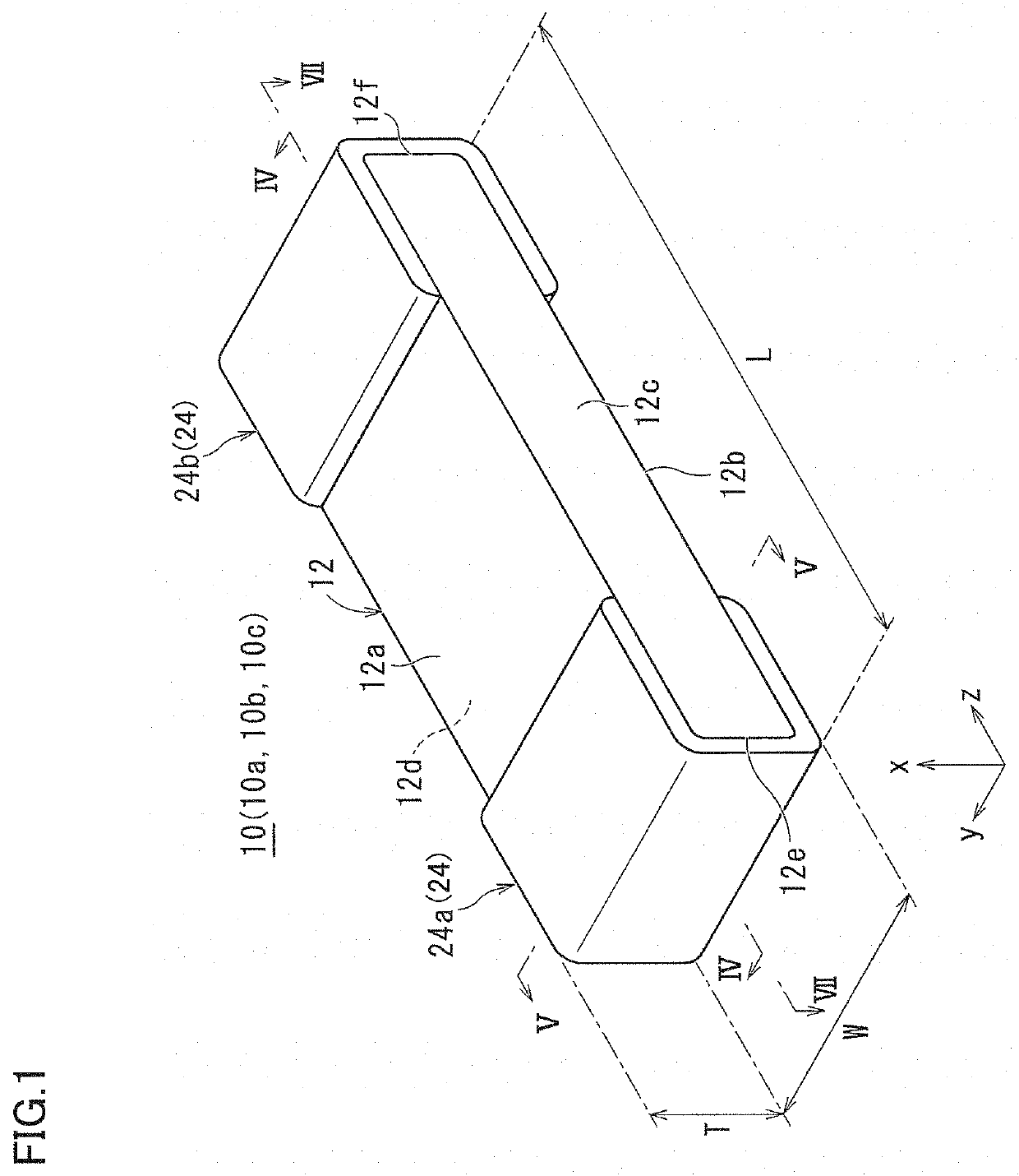
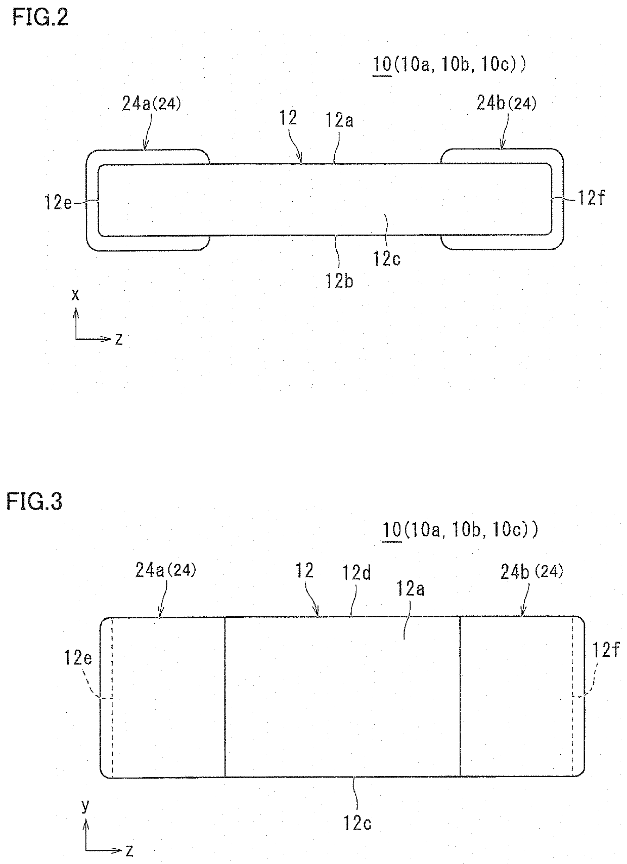
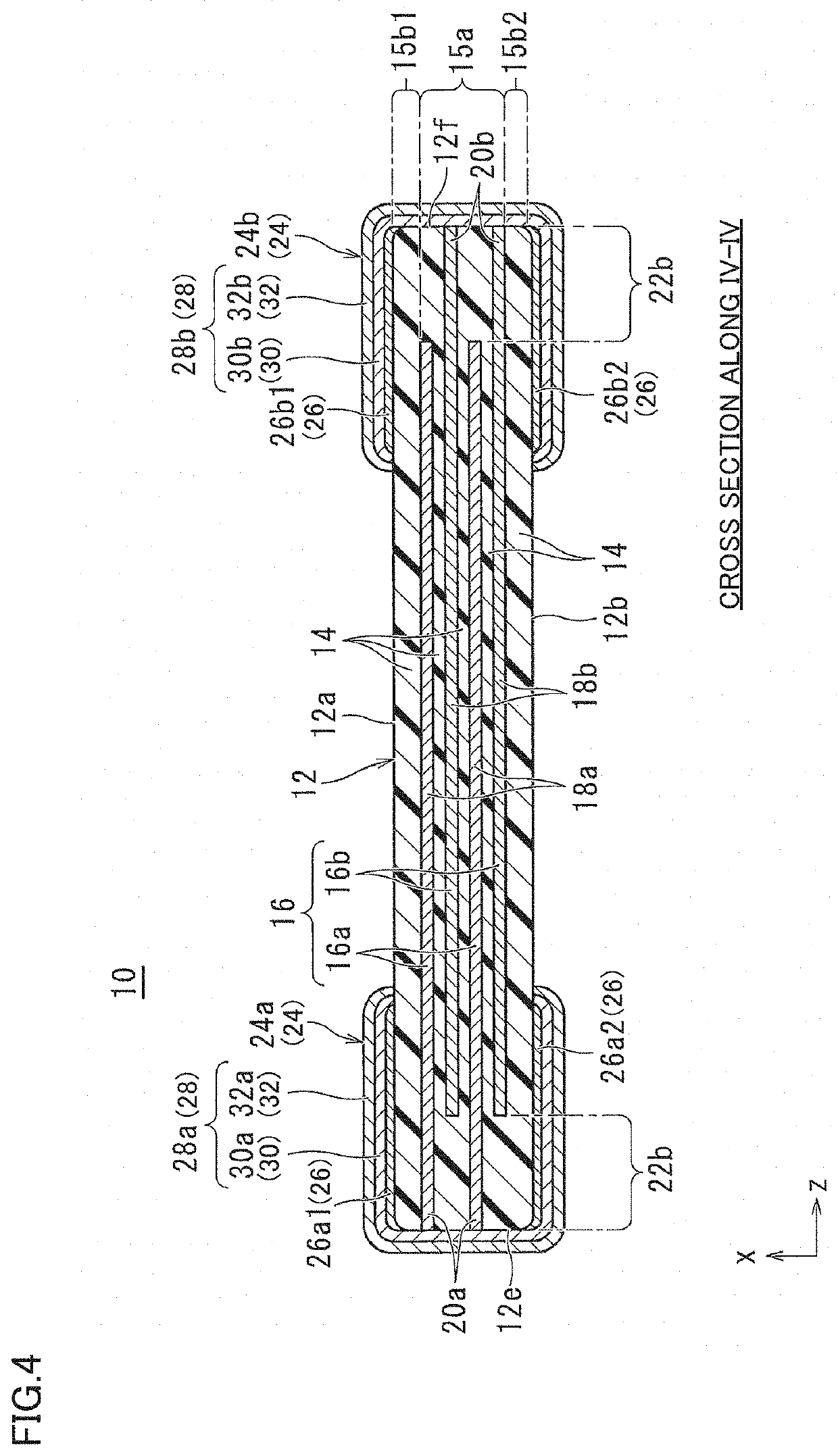
[0044]A multilayer ceramic capacitor 10 which is an example of a multilayer ceramic electronic component according to a first preferred embodiment of the present invention will be described. FIG. 1 is an external perspective view of a multilayer ceramic capacitor as an example of a multilayer ceramic electronic component according to the first preferred embodiment of the present invention. FIG. 2 is a front view of the multilayer ceramic capacitor as the example of the multilayer ceramic electronic component according to the first preferred embodiment of the present invention. FIG. 3 is a top view of the multilayer ceramic capacitor as the example of the multilayer ceramic electronic component according to the first preferred embodiment of the present ...


PUM

PropertyMeasurementUnit
grain diameteraaaaaaaaaa
thicknessaaaaaaaaaa

Abstract

A multilayer ceramic capacitor includes an external electrode including an underlying electrode layer, a lower plating layer on the underlying electrode layer at a first end surface and a second end surface, and an upper plating layer on the lower plating layer. The underlying electrode layer is a thin film electrode including at least one selected from Ni, Cr, Cu, and Ti. The lower plating layer is a Cu plating layer including a lower layer region located closer to the multilayer body and an upper layer region located between the lower layer region and the upper plating layer, and the Cu plating layer in the lower layer region has a metal grain diameter smaller than that of the Cu plating layer located in the upper layer region.

Description

CROSS REFERENCE TO RELATED APPLICATIONS[0001]This application claims the benefit of priority to Japanese Patent Application No. 2020-074660 filed on Apr. 20, 2020. The entire contents of this application are hereby incorporated herein by reference.BACKGROUND OF THE INVENTION1. Field of the Invention[0002]The present invention relates to a multilayer ceramic electronic component, and more particularly, to a multilayer ceramic electronic component including an external electrode with a multilayer structure.2. Description of the Related Art[0003]In recent years, electronic devices such as mobile phones and portable music players are increasingly reduced in size and thickness. Along with this, multilayer ceramic electronic components mounted in such electronic devices are also increasingly reduced in size and thickness.[0004]A multilayer ceramic capacitor that is an example of such a multilayer ceramic electronic component includes, for example, a ceramic sintered body in which a dielec...

Claims


Application Information

Patent Timeline
Patent Type & Authority Applications(United States)
IPC IPC(8): H01G4/30H01G4/012H01G4/008H01G4/232H01G4/12
CPCH01G4/30H01G4/012H01G4/12H01G4/232H01G4/008H01G4/252H01G4/2325H01G4/0085H01G4/1218H01G4/1236
Inventor MURAMATSU, SATOSHITOMINAGA, KEN
Owner MURATA MFG CO LTD
Why Eureka
Try Eureka