Method of making a precision punch and die design and construction

a technology of precision punching and die design, applied in the direction of metal working apparatus, manufacturing tools, cutting tools, etc., can solve the problems of limiting the speed and size of the system, increasing the density of circuits on a single vlsi chip, and increasing the difficulty of achieving the interconnection of vlsi chips in a limited spa

Inactive Publication Date: 2000-09-19
IBM CORP
View PDF10 Cites 26 Cited by
  • Summary
  • Abstract
  • Description
  • Claims
  • Application Information

AI Technical Summary

Benefits of technology

FIG. 8 is a side elevational view of the precision tooling device illustrating first and third die plates positioned on the front side of a first support plate and none on the back side.
FIG. 9 is a side elevational view of the precision tooling device illustrating a first die plate positioned in between a substrate and a first support plate, second and third die plates positioned in between a second support plate and a substrate with the second die plate adjacent to the second support plate and a fourth die plate on the back side of the first support plate.
FIG. 10 is a side elevational view of the precision tooling device illustrating a first die plate in between a first support plate and a substrate, a second die plate in between a second support plate and the substrate, a third die plate on the back side of the first support plate and an air passage between the perimeter of the second support plate and the opening in the second support plate.
FIG. 11 is a perspective view of the second support plate of FIG. 10 illustrating etched air passages connecting the precision holes.
FIG. 12 is a fragmentary view of a section of the second support plate along line 12--12 of FIG. 11, greatly enlarged to show the connection of the air passage from the perimeter of the second support plate to the openings in the second support plate.
FIG. 13 is a greatly enlarged side elevational view of the punch assembly.

Problems solved by technology

The use of VLSI circuits present interface problems relating to the interconnection of the integrated circuits to other circuits and the placement of the integrated circuits on a ceramic circuit board (MCM-C).
As VLSI technology has advanced, the density of circuits on a single VLSI chip has increased and the necessary interconnection for VLSI chips has become increasingly difficult to achieve in a limited space.
The MCM-C packaging limits the speed and size of a system.
The precision of the tooling is the limiting factor in providing a precision punched substrate.
These tool steel plates are heavy, expensive and require sharpening.
The sharpening is time consuming and can only be done several times before the die must be replaced due to wear.

Method used


Image

  • Method of making a precision punch and die design and construction
  • Method of making a precision punch and die design and construction
  • Method of making a precision punch and die design and construction

Examples


Embodiment Construction

)

In describing the preferred embodiment of the present invention, reference will be made herein to FIGS. 1-13 of the drawings in which like numerals refer to like features of the invention. Features of the invention are not necessarily shown to scale in the drawings.

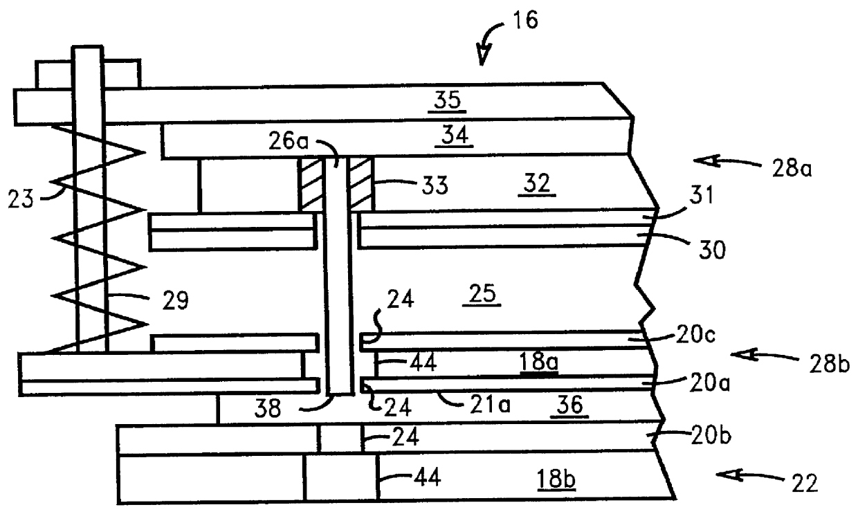
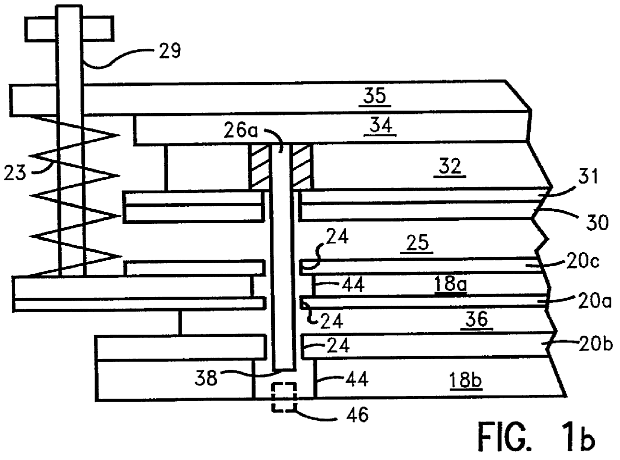
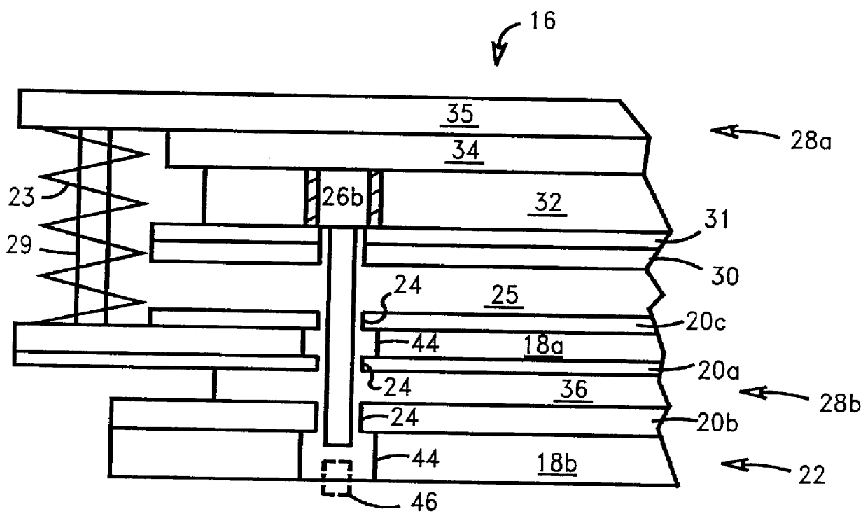
In FIG. 1a there is shown a first embodiment of a precision tooling device 16 which comprises a punch 26a, first and second punch assemblies 28a,b and a die assembly 22. The punch is coaxially aligned with the die and support plate openings of each assembly. The first punch assembly 28a is assembled by layering, from bottom to top, a punch holder mask or die plate 30, a punch holder mask subplate 31, a punch holder insert 32, a punch holder spacer plate 34 and a punch holder back-up plate 35. This first punch assembly 28a configuration is preferred for all embodiments of the present invention. The unheaded punch 26a is fixed in the punch holder insert plate 32. The second punch assembly 28b is assembled by layering from ...


PUM

PropertyMeasurementUnit
sizeaaaaaaaaaa
diameteraaaaaaaaaa
thicknessaaaaaaaaaa

Abstract

A precision punch and die device for punching holes in a ceramic substrate and method of assembling the device. The device comprises a punch which moves relative to the substrate for punching a hole in the substrate and a die assembly including one or more precision die plates and support plates for guiding the punch and punching the substrate.

Description

1. Field of the InventionThis invention relates to an apparatus for punching precision holes and in particular a device for punching precision holes in material used for mounting multiple integrated circuits and for creating holes used for interchip connections in the precision punched material.2. Description of Related ArtCircuit boards with multiple VLSI circuit chips are called Multichip Modules (MCM). The use of VLSI circuits present interface problems relating to the interconnection of the integrated circuits to other circuits and the placement of the integrated circuits on a ceramic circuit board (MCM-C). As VLSI technology has advanced, the density of circuits on a single VLSI chip has increased and the necessary interconnection for VLSI chips has become increasingly difficult to achieve in a limited space. An MCM-C design object is to increase the ratio of the total area occupied by silicon to the total board area, called silicon efficiency ratio. The MCM-C packaging limits ...

Claims


Application Information

Patent Timeline
Patent Type & Authority Patents(United States)
IPC IPC(8): B23P15/24B26F1/02B26D7/18H05K3/00
CPCB23P15/24B26D7/1854B26F1/02B26F2210/08H05K3/0044Y10T83/944Y10T83/9428Y10T83/2172Y10T83/9425Y10T83/8785Y10T83/9437
Inventor DIMARIA, FERDINAND D.
Owner IBM CORP
Why Eureka
Try Eureka