Fabrication of single absorber layer radiated energy conversion device

a technology of radiated energy and absorber layer, which is applied in the manufacturing of semiconductor/solid-state devices, semiconductor devices, electrical devices, etc., can solve the problems of limiting the efficiency effect and making the control of radiation damage more difficul

Inactive Publication Date: 2001-01-30
INTERFACE STUDIES
View PDF47 Cites 86 Cited by
  • Summary
  • Abstract
  • Description
  • Claims
  • Application Information

AI Technical Summary

Problems solved by technology

There are however, in such a device, interrelated structural features that both produce and extract the electrical energy together with reflective mechanisms that operate to get more than one pass out of the radiated energy in hole-electron pair production that, heretofore in the art, required tradeoffs that had a limiting effect on efficiency and made control of radiation damage more difficult.

Method used


Image

  • Fabrication of single absorber layer radiated energy conversion device
  • Fabrication of single absorber layer radiated energy conversion device

Examples


Embodiment Construction

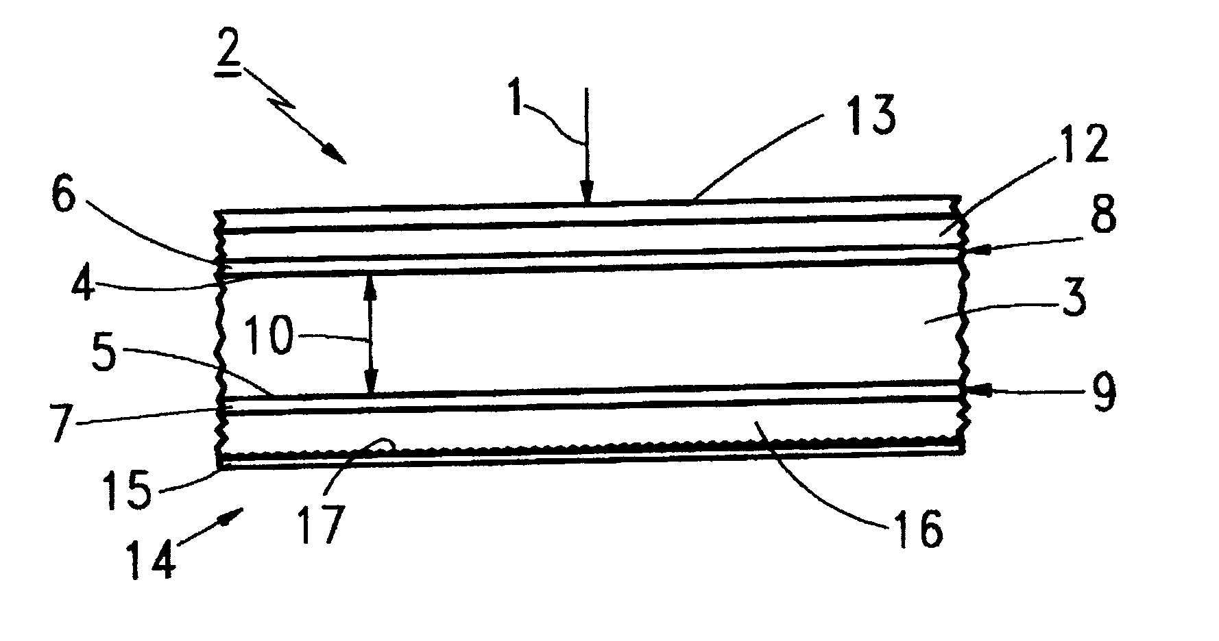
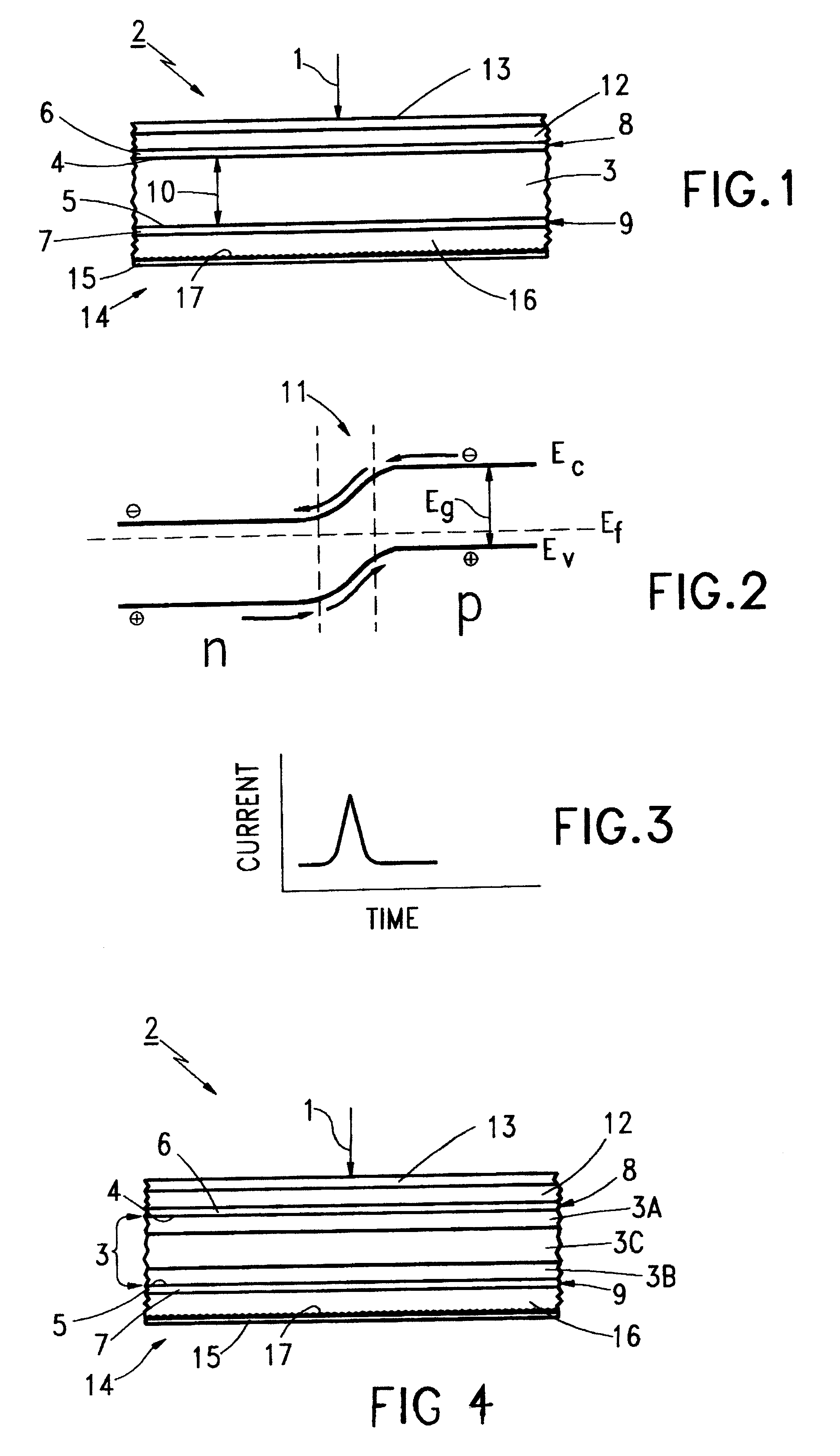
In accordance with the invention it has been found that the efficient absorption of incident radiated energy in a single absorber layer semiconductor device is influenced by a greater number of interrelated factors in different ranges than had been appreciated and employed heretofore in the art. It had heretofore been accepted that since the radiated energy contains a distribution of photon / particles with different energy content, in order to extract a practical amount of energy, it was desirable to have an absorber that had a thickness approaching the full carrier diffusion length. However, the closer to the diffusion length assumed to be needed for thickness, the higher will be the required quality of the semiconductor material. In contrast, in accordance with the invention it has been found that most of the absorption takes place essentially adjacent to the incident radiated energy entrant surface, that in such a thin region there is greater tolerance for semiconductor material d...


PUM


Abstract

A radiated energy to electrical energy conversion device and technology is provided where there is a single absorber layer of semiconductor material. The thickness of the absorber layer is much less than had been appreciated as being useful heretofore in the art. Between opposing faces the layer is about ½ or less of the carrier diffusion length of the semiconductor material which is about 0.02 to 0.5 micrometers. The thickness of the absorber layer is selected for maximum electrical signal extraction efficiency and may also be selected to accommodate diffusion length damage over time by external radiation.

Description

Cross reference is made to the following copending applications that are in the general field of this invention: application Ser. No. 08 / 179,601 filed Jan. 10, 1994 of John L. Freeouf titled "Solid State Radiation Detector" and application Ser. NO. 09 / 034,430 filed Mar. 3, 1998 titled "Multi Absorber Layer Radiated Energy To Electrical Energy Conversion Device" and assigned to the assignee of this invention.The invention relates to a highly efficient, single semiconductor absorption layer, radiated energy conversion device in which there is also provision for accommodation for performance degradation resulting from exposure to external radiation.BACKGROUND OF THE INVENTION AND RELATION TO THE PRIOR ARTIn the conversion of radiated energy to electrical energy, it has been the practice in the art to use solid state semiconductor layer structures that can produce hole-electron pairs that result from atomic particles or photons, in passing through the semiconductor, engaging in primary ...

Claims


Application Information

Patent Timeline
Patent Type & Authority Patents(United States)
IPC IPC(8): H01L31/06
CPCH01L31/06Y02E10/50
Inventor FREEOUF, JOHN LAWRENCE
Owner INTERFACE STUDIES
Why Eureka
Try Eureka