Integration of ALD/CVD barriers with porous low k materials

a technology of low k materials and barriers, applied in the field of metal interconnect structure formation, can solve the problems of reducing affecting the reliability affecting the quality of the overall circuit,

Active Publication Date: 2004-12-23
APPLIED MATERIALS INC
View PDF99 Cites 120 Cited by
  • Summary
  • Abstract
  • Description
  • Claims
  • Application Information

AI Technical Summary

Problems solved by technology

However, copper diffuses more readily into surrounding materials and can alter the electronic device characteristics of the adjacent layers.
For example, such diffusion can form a conductive path between layers, thereby reducing the reliability of the overall circuit and possibly cause device failure.
The addition of the barrier layer on the bottom of the feature not only increases the overall resistance of the feature, but also forms an obstruction between higher and lower metal interconnects of a multi-layered interconnect structure.
As with the diffusion of copper discu

Method used


Image

  • Integration of ALD/CVD barriers with porous low k materials
  • Integration of ALD/CVD barriers with porous low k materials
  • Integration of ALD/CVD barriers with porous low k materials

Examples


Embodiment Construction

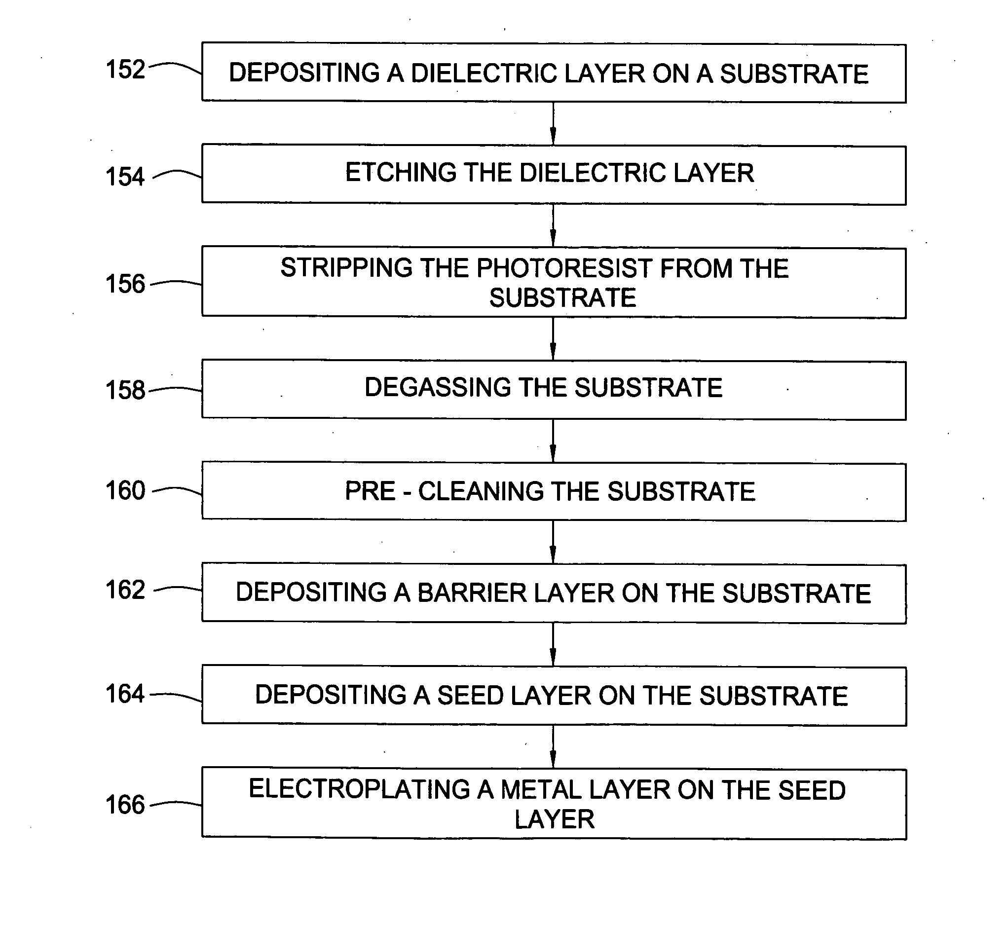
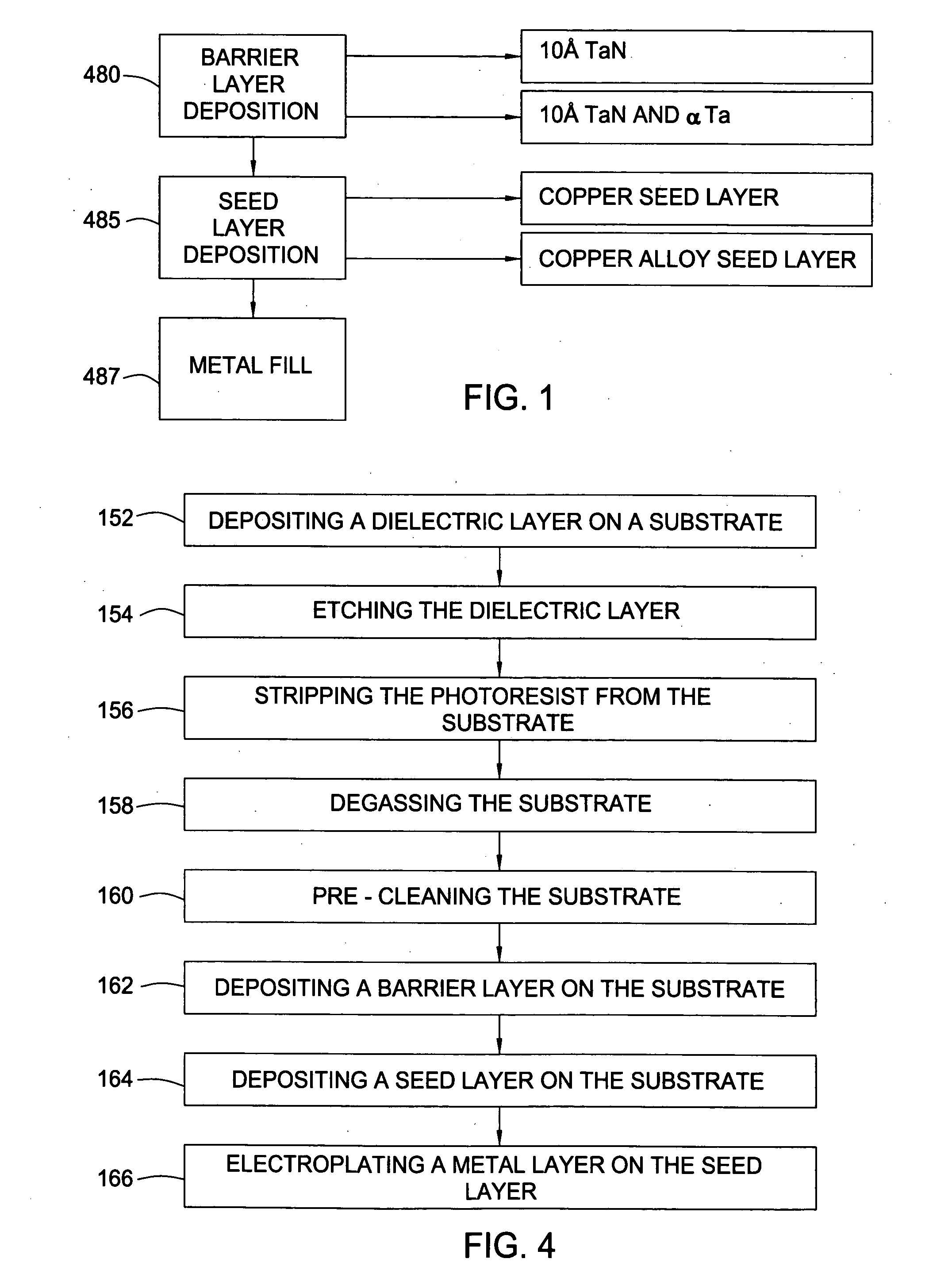
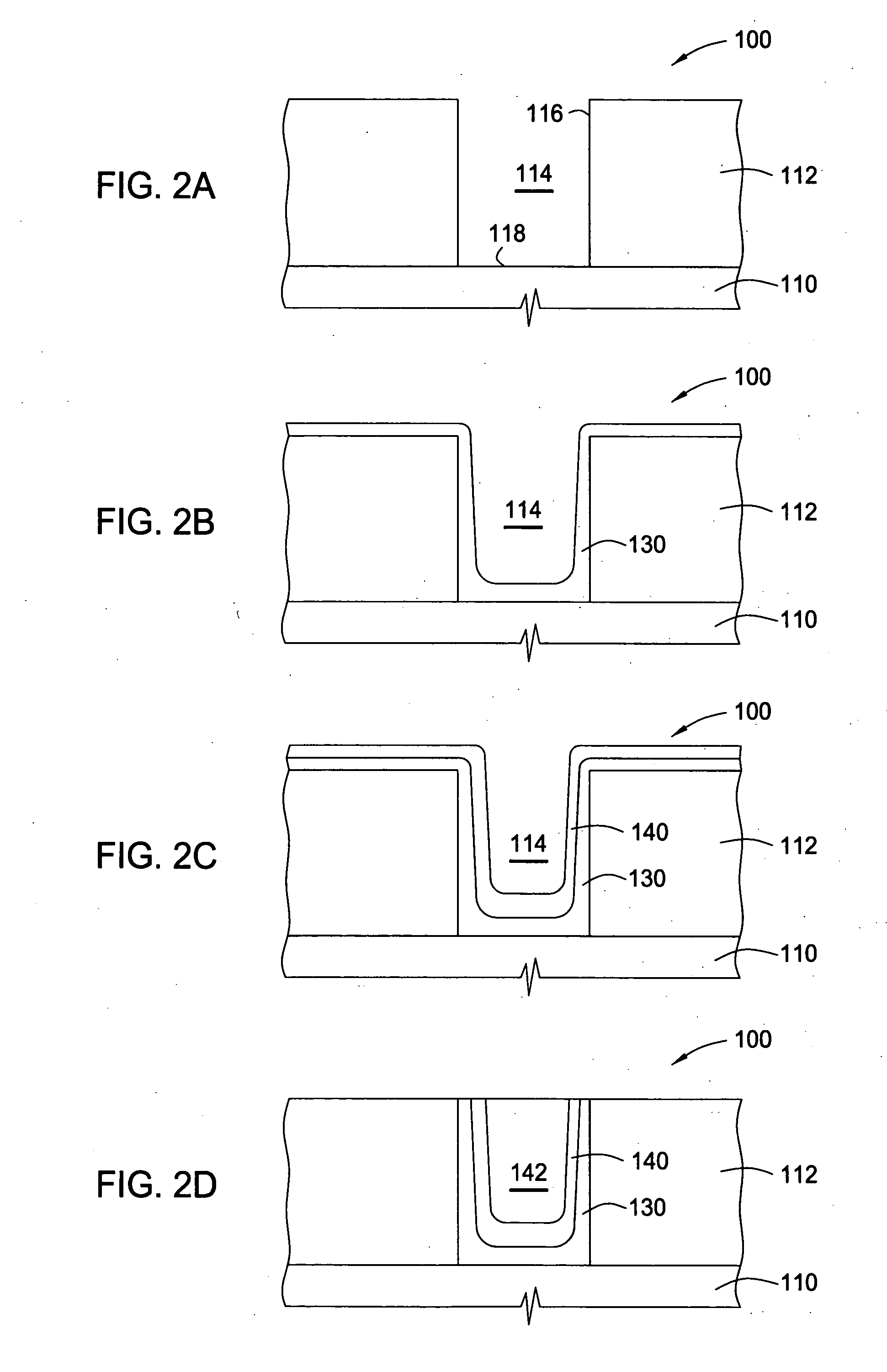
[0099] An extremely low k (k<3) dielectric layer was deposited on a substrate. The dielectric layer was then etched to form a feature, such as a hole, therein, and an etch stop layer at the bottom of the feature is also at least partially etched. The substrate was degassed at 350.degree. C. for about 100 seconds. The substrate was pre-cleaned in a Pre-Clean II chamber under the following conditions: 300 W of RF power was applied to the coil surrounding the chamber, a RF bias of 300 W was applied to the substrate support member supporting the substrate, and the substrate was pre-cleaned with an argon plasma for about 23 seconds. A TaN barrier layer was then deposited on the substrate from a sequential exposure of PDMAT and NH.sub.3. The TaN barrier layer was deposited by first introducing argon into the chamber at 100 sccm for 0.1 seconds, and then alternately pulsing NH.sub.3 at 1000 sccm for 1 second and PDMAT carried in an argon flow of 100 sccm for 0.5 seconds, with a flow of arg...


PUM

PropertyMeasurementUnit
Timeaaaaaaaaaa
Timeaaaaaaaaaa
Poweraaaaaaaaaa

Abstract

A method for processing substrates is provided. The method includes depositing and etching a low k dielectric layer on a substrate, pre-cleaning the substrate with a plasma, and depositing a barrier layer on the substrate. Pre-cleaning the substrate minimizes the diffusion of the barrier layer into the low k dielectric layer and/or enhances the deposition of the barrier layer.

Description

[0001] This application claims benefit of U.S. provisional patent application Ser. No. 60 / 438,480, filed Jan. 7, 2003, which is herein incorporated by reference.[0002] 1. Field of the Invention[0003] Embodiments of the present invention relate to a method for manufacturing integrated circuit devices. More particularly, embodiments of the invention relate to forming metal interconnect structures having a barrier layer contacting at least a part of a dielectric layer.[0004] 2. Description of the Related Art[0005] As the structure size of integrated circuit (IC) devices is scaled down to sub-quarter micron dimensions, electrical resistance and current densities have become an area for concern and improvement. Multilevel interconnect technology is used to form high aspect ratio features, including contacts, plugs, vias, lines, wires, and other features. A typical process for forming an interconnect on a substrate includes depositing one or more layers, etching at least one of the layer(...

Claims


Application Information

Patent Timeline
IPC IPC(8): C23C16/34H01B13/00H01L21/285H01L21/306H01L21/311H01L21/768
CPCC23C16/34H01L21/02063H01L21/28556H01L21/28562H01L21/31116H01L21/76876H01L21/76814H01L21/76838H01L21/76843H01L21/76873H01L21/76802
Inventor CHUNG, HUABEKIARIS, NIKOLAOSMARCADAL, CHRISTOPHECHEN, LING
Owner APPLIED MATERIALS INC
Why Eureka
Try Eureka